Wiring board

a wiring board and wire technology, applied in the field of wiring boards, can solve the problems of increasing risk, affecting the quality of finished products, and the length of all the bus wiring paths cannot be completely equal, so as to reduce the difference in signal transmission delay

Active Publication Date: 2010-06-01
RENESAS ELECTRONICS CORP
View PDF10 Cites 9 Cited by
  • Summary
  • Abstract
  • Description
  • Claims
  • Application Information

AI Technical Summary

Benefits of technology

[0014]According to the present invention, it is possible to set path lengths from the first semiconductor chip to the second to 2n+1th semiconductor chips to be completely equal including the lengths of the vias and also to minimize a difference in delay of signal transmission due to the wiring within the board.

Problems solved by technology

However, according to the conventional technology, the lengths of all the bus wiring paths cannot be set completely equal since some include the lengths of the vias while other do not.
Therefore, there is a difference in delay of signal transmission among the wiring paths within the board.
As a result, there is an increasing risk that a stable operation cannot be guaranteed in an operation beyond the gigabit speed.

Method used


Image

  • Wiring board
  • Wiring board
  • Wiring board

Examples


example 1

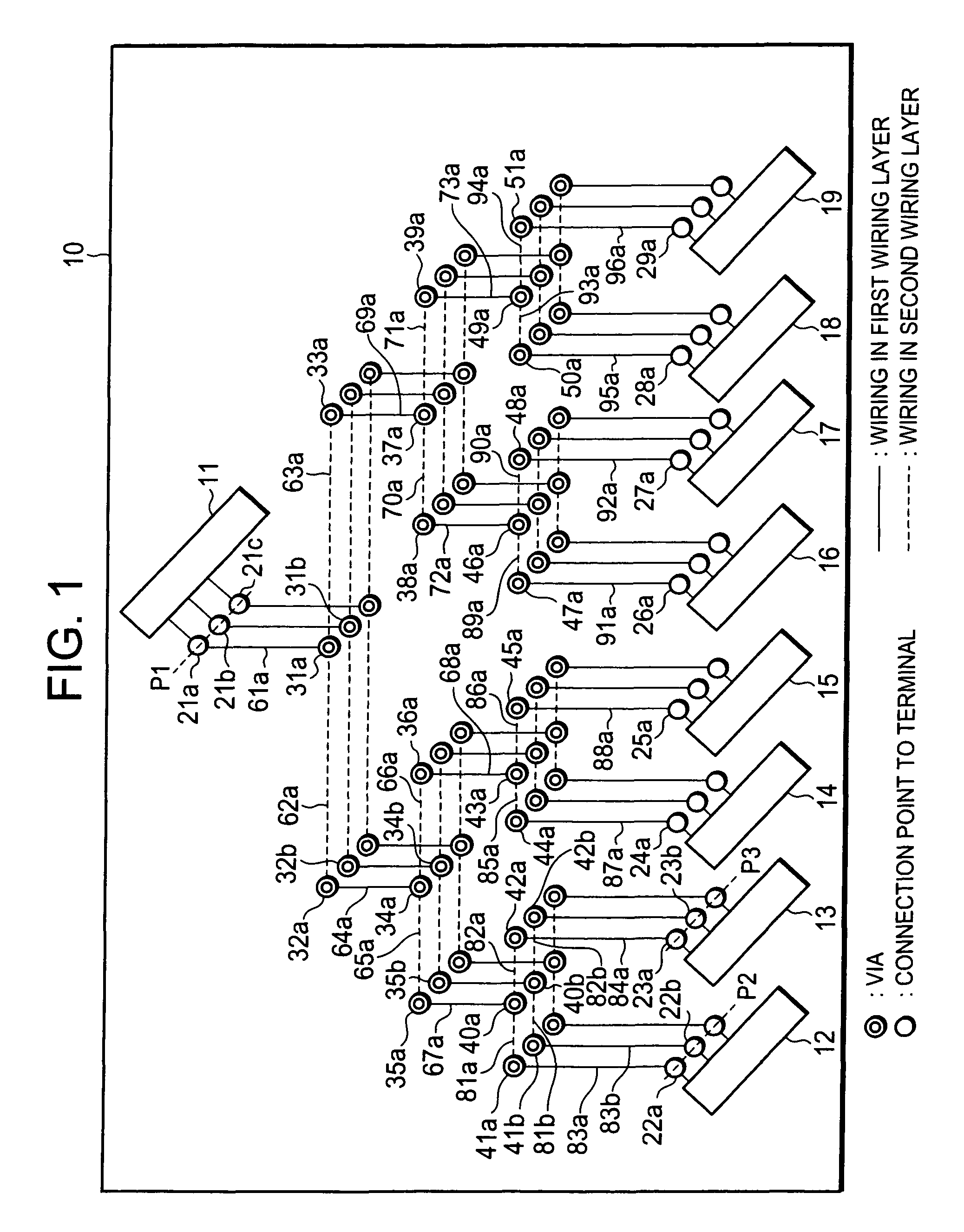
[0025]FIG. 1 is a view schematically showing a structure of a wiring board according to a first example of the present invention. Here, FIG. 1 shows an example of the case where n=3. In FIG. 1, a wiring board 10 has at least first and second wiring layers (for example, front-side and back-side layers) and can mount semiconductor chips 11 to 19. For example, the semiconductor chip 11 is a memory controller and the semiconductor chips 12 to 19 are RAMs controlled by the memory controller. The wiring board 10 includes wires for connecting terminals included in the respective semiconductor chips 11 to 19 to each other through branch points. Here, the wiring from the semiconductor chip 11 to the semiconductor chips 12 to 19 form a complete binary tree structure in which all leaves are at the same depth from a root.

[0026]For example, in the wiring up to a connection point (pad) 21a for the terminals of the semiconductor chip 11, the connection point 21a is connected to a second layer end ...

example 2

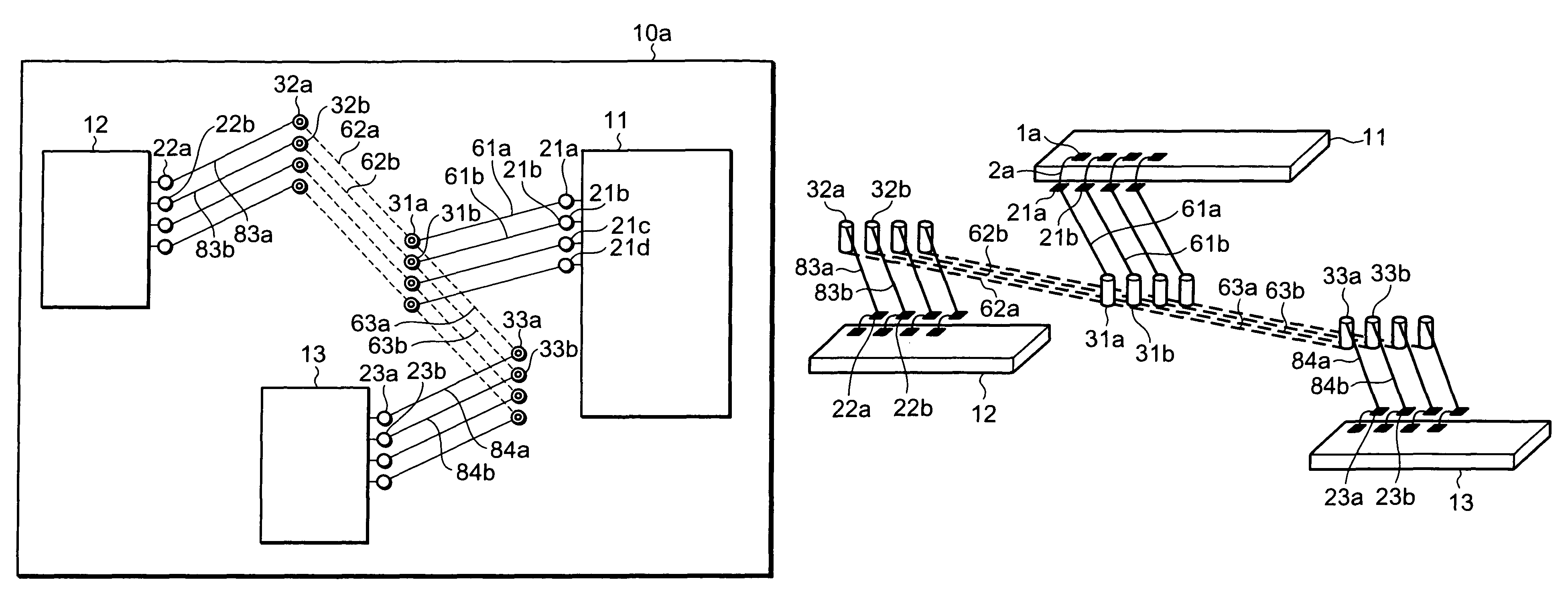
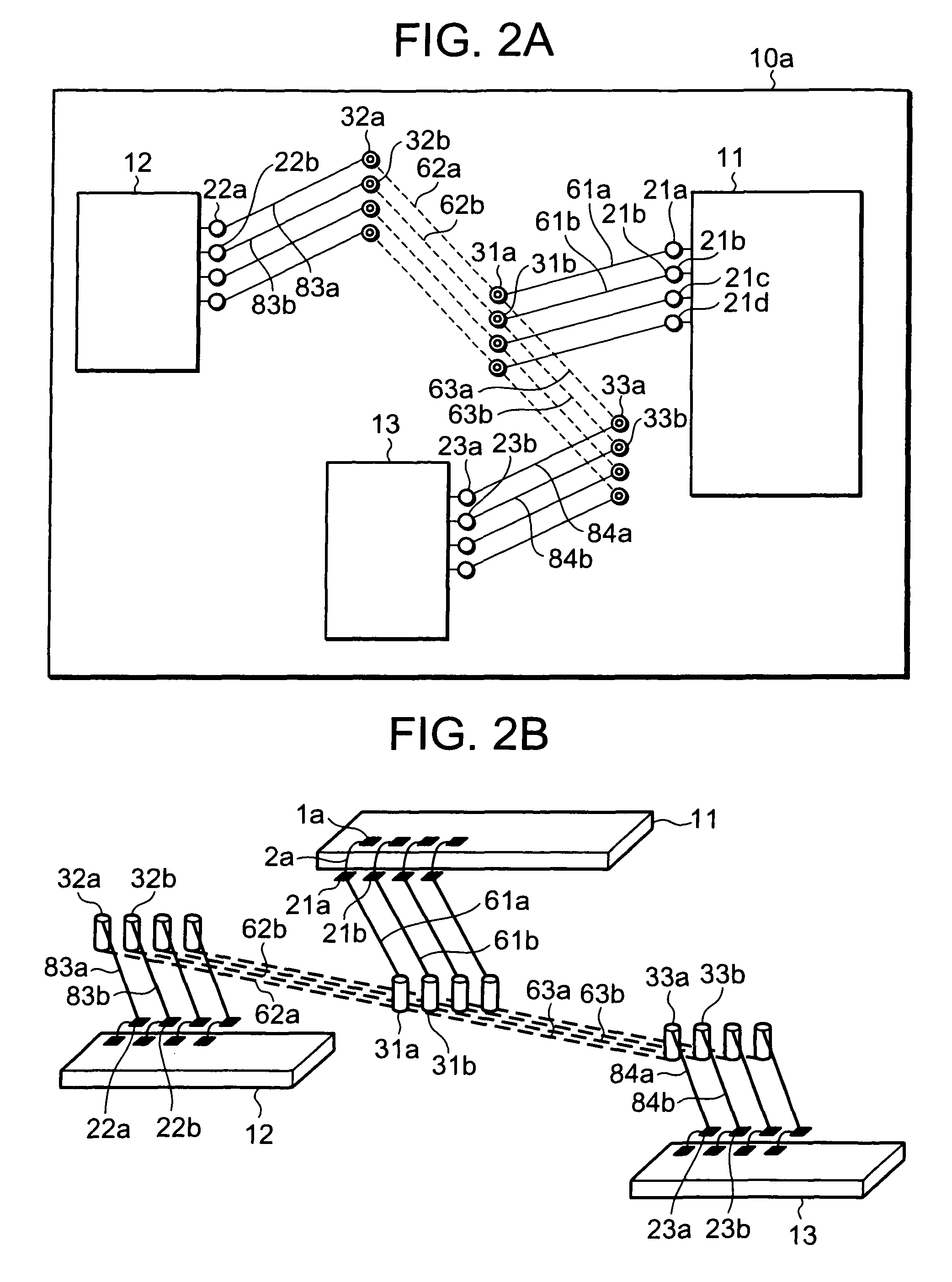
[0050]FIGS. 2A and 2B are views schematically showing a structure of a wiring board according to a second example of the present invention. FIG. 2A is a plan view and FIG. 2B is a perspective view showing a wiring board 10a. Here, FIGS. 2A and 2B show an example of the case where n=1. In FIGS. 2A and 2B, the same reference numerals as those in FIG. 1 represent the same elements and description thereof will be omitted.

[0051]In FIG. 2B, a wire is provided between a terminal (bonding pad) 1a of a semiconductor chip 11 and a connection point (pad) 21a by use of a bonding wire 2a. For connection points (pads) 21b to 21d, wires are similarly provided. Moreover, for semiconductor chips 12 and 13, wires are similarly provided. Note that reference numerals for the wiring up to the connection points 21c and 21d are omitted to simplify the illustration.

[0052]The wiring up to the connection point 21a, the wiring up to the connection point 21b, the wiring up to the connection point 21c and the w...


PUM


Abstract

A difference in delay of signal transmission due to the wiring within a board is minimized. A wiring board includes wiring for connecting terminals included in one of a plurality of semiconductor chips to terminals included in another one of the plurality of semiconductor chips, through branch points. Each of the plurality of semiconductor chips includes first and second terminals. Moreover, a first wiring up to the first terminals and a second wiring up to the second terminals are in a positional relationship of being shifted parallel to each other in a planar direction of the wiring board so as not to come into electrical contact with each other. In each of the first and second wirings, a wire is provided between a connection point for the terminal in a first one of the semiconductor chips and a position of a root, a complete binary tree structure in which all leaves are at the same depth from the root is formed, connection points for the terminals in the rest of the semiconductor chips are positioned at the respective leaves, and the paths of wires respectively corresponding to branches at the same depth in the tree structure include vias and the lengths of the paths of wires including the lengths of the vias are equal to each other.

Description

BACKGROUND OF THE INVENTION[0001]1. Field of the Invention[0002]The present invention relates to a wiring board and more particularly relates to a wiring board including wiring for connecting terminals included in one of a plurality of semiconductor chips to terminals included in another one of the plurality of semiconductor chips, through branch points.[0003]2. Description of the Related Art[0004]There are a wide variety of electronic devices that implement one-to-many connection between a plurality of semiconductor chips, for example, between one memory controller chip and a plurality of random access memories (hereinafter referred to as RAMs), all of which are mounted on a board. Such boards include a board having a plurality of semiconductor chips or semiconductor modules mounted thereon, such as a semiconductor package board, a printed circuit board, a system-in-package board and a multichip module board.[0005]In the connection between a memory controller chip and a plurality o...

Claims


Application Information

Patent Timeline
Patent Type & Authority Patents(United States)
IPC IPC(8): H01L23/52H01L23/48H01L29/40
CPCH01L23/49838H01L23/66H01L25/18H05K1/181H05K2201/09227H05K2201/09254H01L2924/0002H05K2201/09627H05K2201/10159H01L2924/00Y02P70/50
Inventor HAYASHI, AKIMORI
Owner RENESAS ELECTRONICS CORP
Why Eureka
Try Eureka