Voltage control circuit, a voltage control method and a semiconductor memory device having the voltage control circuit

a voltage control circuit and voltage control technology, applied in static storage, digital storage, instruments, etc., can solve the problems of reducing the size of the other transistor controlling the core, exhibiting process defects, and reducing the area efficiency of other transistors, so as to improve the performance of the core, enhance the area efficiency, and enhance the effect of area efficiency

Active Publication Date: 2010-06-01
SK HYNIX INC
View PDF6 Cites 8 Cited by
  • Summary
  • Abstract
  • Description
  • Claims
  • Application Information

AI Technical Summary

Benefits of technology

[0016]The present invention also provides a semiconductor memory device that enhances area efficiency of other transistors which are used for controlling the core by arranging the voltage control circuit in a peripheral region, thereby improving performance of the core.
[0017]The present invention provides a semiconductor memory device with enhanced area efficiency that enables eliminating a metal line used for providing the bleed voltage by arranging the above-mentioned voltage control circuit.

Problems solved by technology

Such semiconductor memory devices exhibit process defects such as a gate residue, which leads to producing a resistive short in the word line and in the bit line and in generating a current path.
According to such prior art, since the voltage control circuit 1 is arranged in the core region, there is a problem in that the size of the other transistor controlling the core is reduced, which can result in decreasing the performance of the core.
Moreover, considering that, for example, a metal pitch is 1.2 μm, the number of a sense amp array is 33 per bank, and there are 4 banks with respect to a metal line 6 arranged to apply the bleed voltage VBLEED, a problem can occur when a length of the metal line 6 is increased by 80 μm and thus the total area of the semiconductor memory device is increased.
Further, since the voltage control circuit 1 can not control the bleed voltage VBLEED, it is difficult to satisfy an amount of leakage current required for certain specification, thereby reducing product yield of the semiconductor memory device.
For example, if the amount of leakage current in the standby state can not satisfy specification defined in IDD2P, it is difficult to control the bleed voltage VBLEED, which results in poor yield of the semiconductor memory device.
Since the bleed voltage VBLEED lower than the precharge voltage VBLP is applied as the precharge voltage irrespective of the active state and the standby state, then the time to precharge the bit lines BL, BLB in the active state is increased, which necessarily results in lowering the precharge performance.

Method used


Image

  • Voltage control circuit, a voltage control method and a semiconductor memory device having the voltage control circuit
  • Voltage control circuit, a voltage control method and a semiconductor memory device having the voltage control circuit
  • Voltage control circuit, a voltage control method and a semiconductor memory device having the voltage control circuit

Examples


Embodiment Construction

[0040]Hereinafter, preferred embodiments of the present invention will be described in detail with reference to the accompanying drawings.

[0041]The present invention provides a voltage control circuit, a voltage control method and a semiconductor memory device having the voltage control circuit that is configured to provide a voltage, within certain specification limits, as a bit line precharge voltage by searching the voltage which minimizes an amount of leakage current from a bit line to a word line.

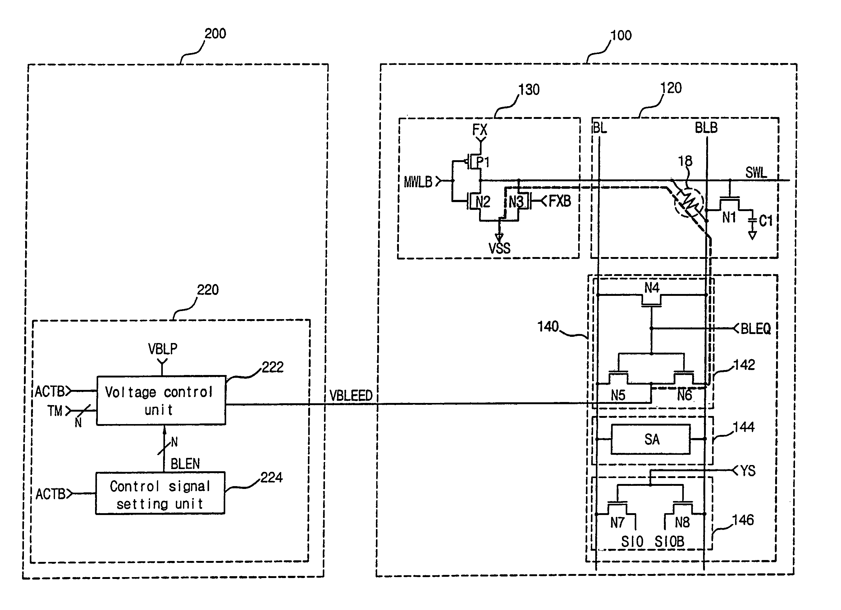
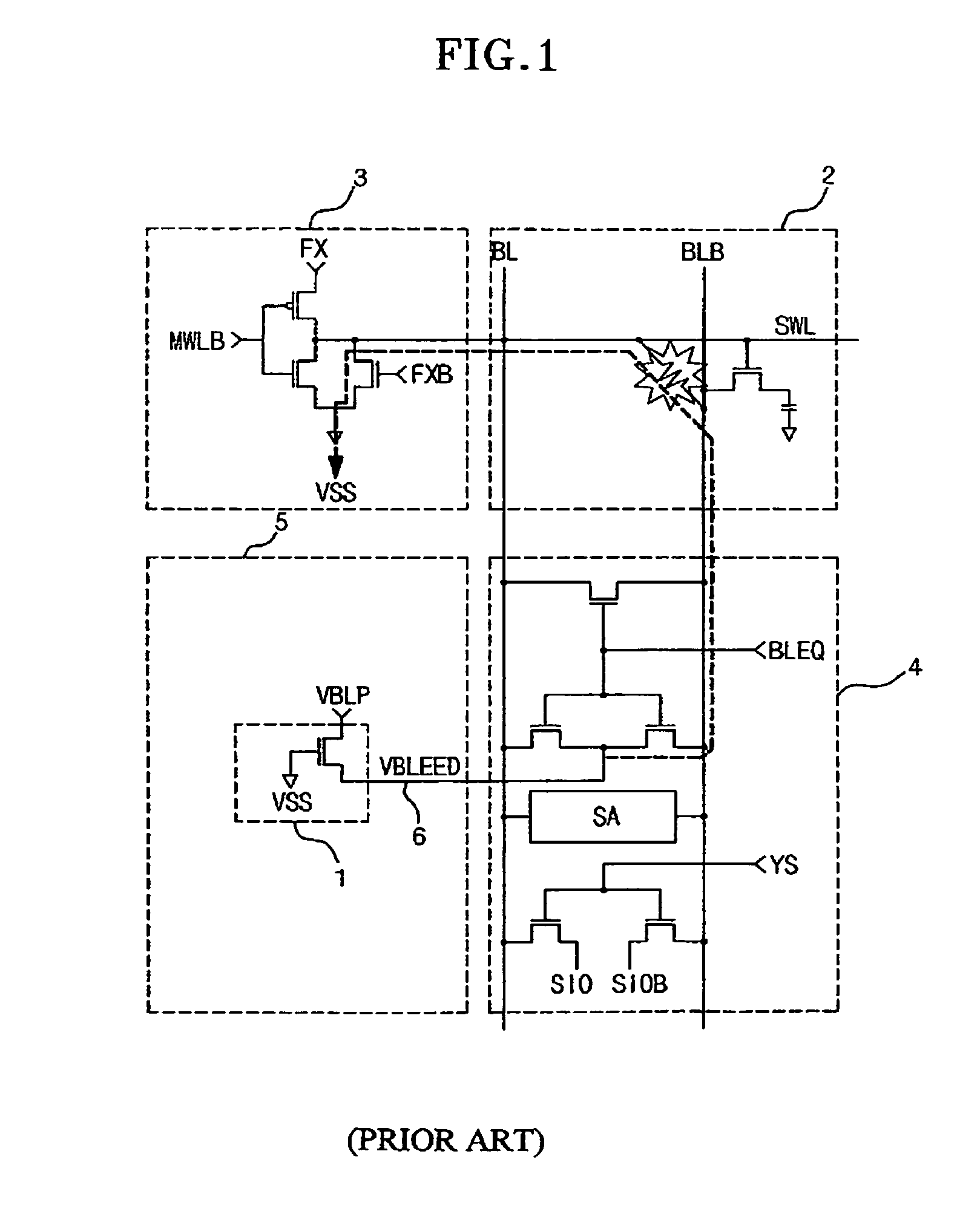
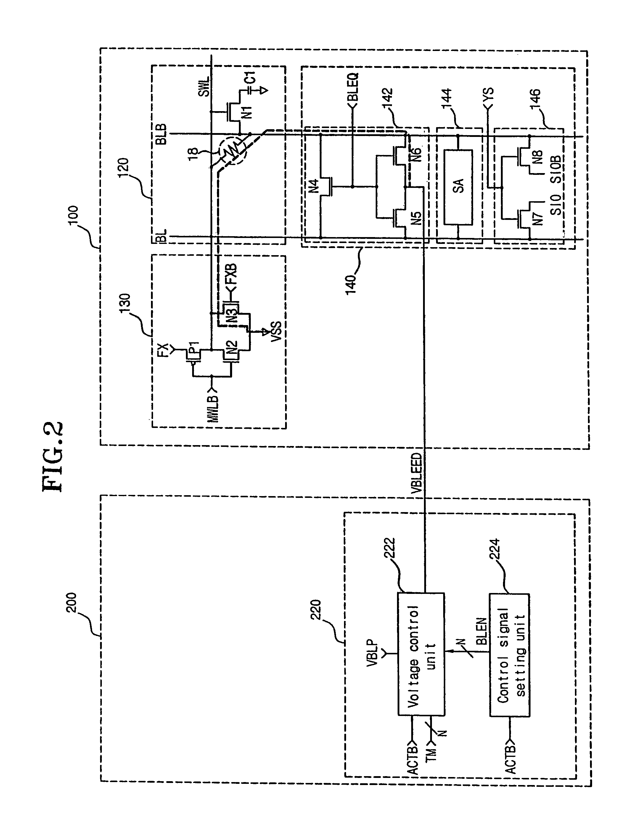
[0042]Referring to FIG. 2, the semiconductor memory device according to an embodiment of the present invention has a bit line (BLB) and a subword line (SWL) short-circuited due to a gate residue so that a current path from the bit line (BLB) to the ground voltage VSS through a subword line (SWL) is formed as shown in thick dotted line of FIG. 2, whereby leakage currents are generated.

[0043]A core region 100 includes a memory cell array unit 120, a subword line driver unit 130, and a se...


PUM


Abstract

A semiconductor memory device includes a voltage control circuit providing different voltages as a precharge voltage in accordance with an active state and a standby stage. The semiconductor memory device is arranged in a peripheral region, whereby the different voltages can be provided as a precharge voltage in accordance with the active state and the standby state and thus leakage current is reduced and area efficiency is enhanced.

Description

CROSS-REFERENCE TO RELATED APPLICATIONS[0001]The present application claims priority to Korean patent application number 10-2006-0129031 filed on Dec. 15, 2006, which is incorporated herein by reference in its entirety.BACKGROUND OF THE INVENTION[0002]The present invention relates to a semiconductor memory device, and more particularly to a voltage control circuit, a voltage control method and a semiconductor memory device having the voltage control circuit which can reduce leakage currents and improve precharge performance.[0003]Generally, a semiconductor memory device enters into an active state in response to an active command and activates a given word line. Subsequently, the semiconductor memory device delivers cell data corresponding to the word line to outside through bit lines or stores the data delivered from outside on the corresponding cell through the bit lines.[0004]When the semiconductor memory device enters a standby state in response to a precharge command, the bit l...

Claims


Application Information

Patent Timeline
Patent Type & Authority Patents(United States)
IPC IPC(8): G11C5/14
CPCG11C5/147G11C7/12G11C11/4094G11C11/4074G11C2207/2227G11C5/148G11C29/02
Inventor XI, SUNG SOO
Owner SK HYNIX INC
Why Eureka
Try Eureka