Socket, and test apparatus and method using the socket

a technology of sockets and sockets, which is applied in the direction of individual semiconductor device testing, semiconductor/solid-state device testing/measurement, instruments, etc., can solve the problems of large amount of time for developing fine pattern forming technology, large amount of time for testing all connection terminals, and large amount of time for above methods to achieve efficient testing of electric characteristics

Active Publication Date: 2010-06-15
SAMSUNG ELECTRONICS CO LTD
View PDF12 Cites 19 Cited by
  • Summary
  • Abstract
  • Description
  • Claims
  • Application Information

AI Technical Summary

Benefits of technology

[0010]In accordance with the present invention, provided is an apparatus and method for efficiently testing electric characteristics of a semiconductor device package, such as electric connection states of the semiconductor device package—including connection terminals on top and bottom surfaces thereof.
[0011]In accordance with the present invention, also provided is an apparatus and method for rapidly testing electric characteristics of a semiconductor package, such as electric connection states of a semiconductor device package—including connection terminals on top and bottom surfaces thereof.
[0012]In accordance with the present invention, also provided is an apparatus and method for testing electric connection states of a multi-chip semiconductor device package that eliminates the possibility of discarding a non-defective upper semiconductor device package according to the test result of a lower semiconductor device package.

Problems solved by technology

However, it is difficult and takes a large amount of time to develop highly integrated memory chips.
However, it is difficult and takes a large amount of time to develop the fine pattern forming technology.
However, the above method takes a large amount of time to test all the connection terminals of the top and bottom surfaces of the first semiconductor device package.
Moreover, even if the second semiconductor device package is not defective, the second semiconductor device package can be discarded if it is determined that the electric characteristics of the connection terminals of the top surface of the first semiconductor device package are not allowable, i.e., defective.

Method used


Image

  • Socket, and test apparatus and method using the socket
  • Socket, and test apparatus and method using the socket
  • Socket, and test apparatus and method using the socket

Examples


first embodiment

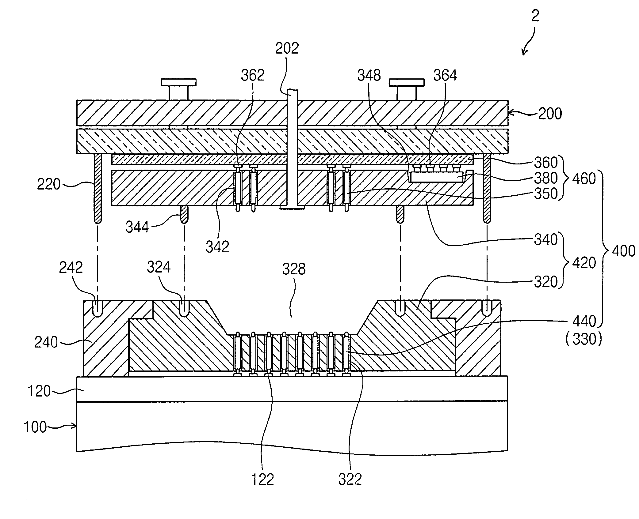
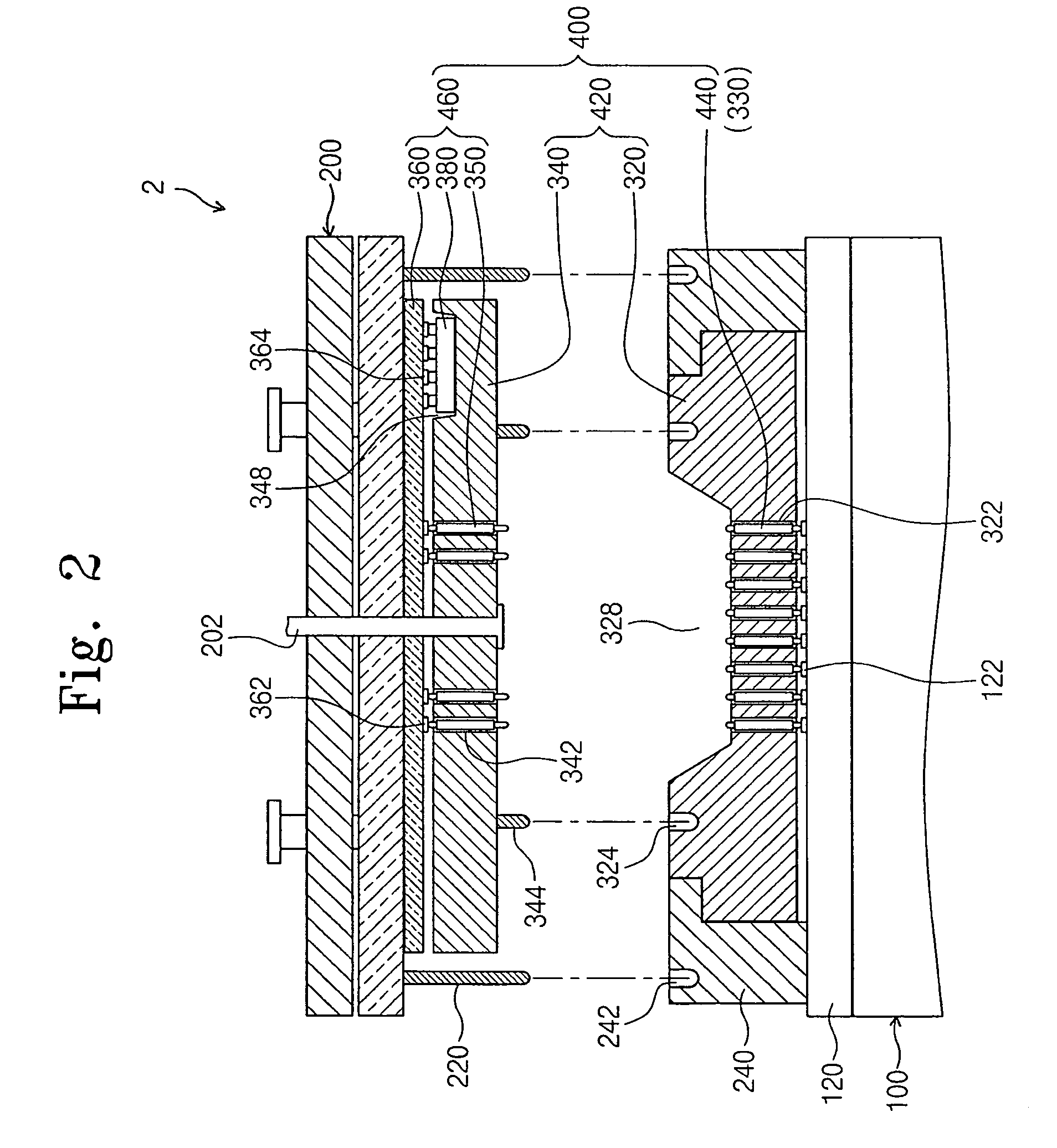
[0065]FIG. 2 is an exploded cross-sectional view illustrating a test apparatus 2 according to an aspect of the present invention, FIG. 3 is a cross-sectional view illustrating the test apparatus 2 assembled for testing the first semiconductor device package 10.

[0066]Referring to FIGS. 2 and 3, the test apparatus 2 includes a test unit 100, a handler 200, and a socket 400. The test unit 100 applies an input signal to the first semiconductor device package 10 (hereinafter, referred to as a test object) and receives a signal output from the test object 10 in response to the input signal. The test unit 100 evaluates the state of the test object 10 using the signal output from the test object 10. The test unit 100 includes a test board 120. First pads 122 are formed on a top surface of the test board 120. Automatic test equipment can be used as the test unit 100. The socket 400 electrically connects the first semiconductor device package 10 to the test board 120. The handler 200 is confi...

second embodiment

[0092]In the second embodiment, the electric connection states of the first connection terminals 14 formed on the bottom surface of the test object 10 can be measured simultaneously with the electric connection states of the second connection terminals 16 formed on the top surface of the test object 10.

[0093]According to aspects of the present invention, the connection states of the connection terminals disposed on the bottom surface of the test object can be tested simultaneously with the connection states of the connection terminals disposed on the top surface of the test object.

[0094]In addition, before the first and second semiconductor device packages are coupled together using solder balls, the first and second semiconductor device packages can be tested under conditions similar to those in a case where the first and second semiconductor device packages are coupled together.


PUM


Abstract

An apparatus for testing electric characteristics of a test object including first connection terminals on a bottom surface and second connection terminals on a top surface, the apparatus comprises a test board comprising first pads on a predetermined surface; a socket configured to electrically connect the test object to the test board; and a handler configured to transport the test object to the socket. The socket comprises a first connection unit configured to be electrically connected to the first connection terminals of the test object and a second connection unit configured to be electrically connected to the second connection terminals of the test object.

Description

CROSS-REFERENCE TO RELATED APPLICATIONS[0001]This U.S. non-provisional patent application claims the benefit of priority under 35 U.S.C. §119 to Korean Patent Application No. 10-2007-0069259, filed on Jul. 10, 2007, the entire contents of which are hereby incorporated by reference.FIELD OF THE INVENTION[0002]The present invention disclosed herein relates to a test apparatus and method, and more particularly, to an apparatus and method for testing electrical characteristics of a semiconductor device package.BACKGROUND[0003]In semiconductor industries, packaging technology has been advanced for increasing reliability in packaging and mounting small-sized integrated semiconductor chips. For example, demands for miniaturization have accelerated the development of small packages having sizes close to the sizes of integrated semiconductor chips, and demands for reliable mounting technology have spurred the development of packaging technology for efficiently packaging semiconductor chips a...

Claims


Application Information

Patent Timeline
Patent Type & Authority Patents(United States)
IPC IPC(8): G01R31/02G01R31/26H01L23/58
CPCG01R1/0483G01R1/0466H01L2224/48091H01L2224/73265H01L2924/00014G01R31/26H01L22/00
Inventor CHO, BYEONG-HWAN
Owner SAMSUNG ELECTRONICS CO LTD
Why Eureka
Try Eureka