
Scheme for controlling rise-fall times in signal transitions

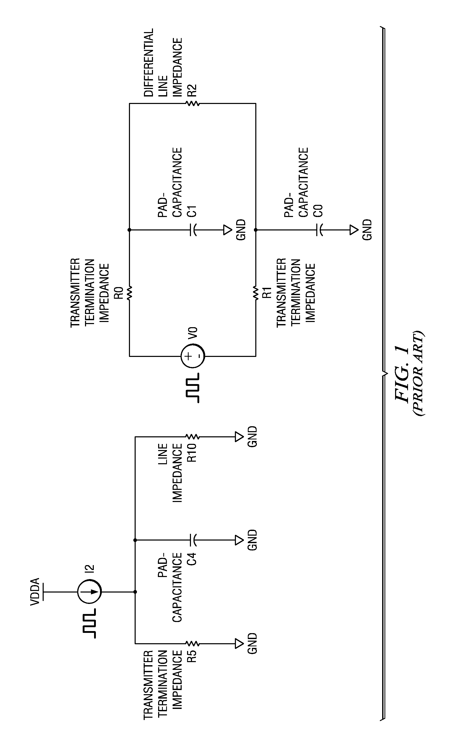
a signal transition and rise-fall time technology, applied in pulse manipulation, pulse technique, baseband system details, etc., can solve the problems of poor receiver performance, too much pad capacitance on the pads, and very small rise-fall tim

Active Publication Date: 2010-06-15
TEXAS INSTR INC
View PDF4 Cites 8 Cited by
  • Summary
  • Abstract
  • Description
  • Claims
  • Application Information

AI Technical Summary

Benefits of technology

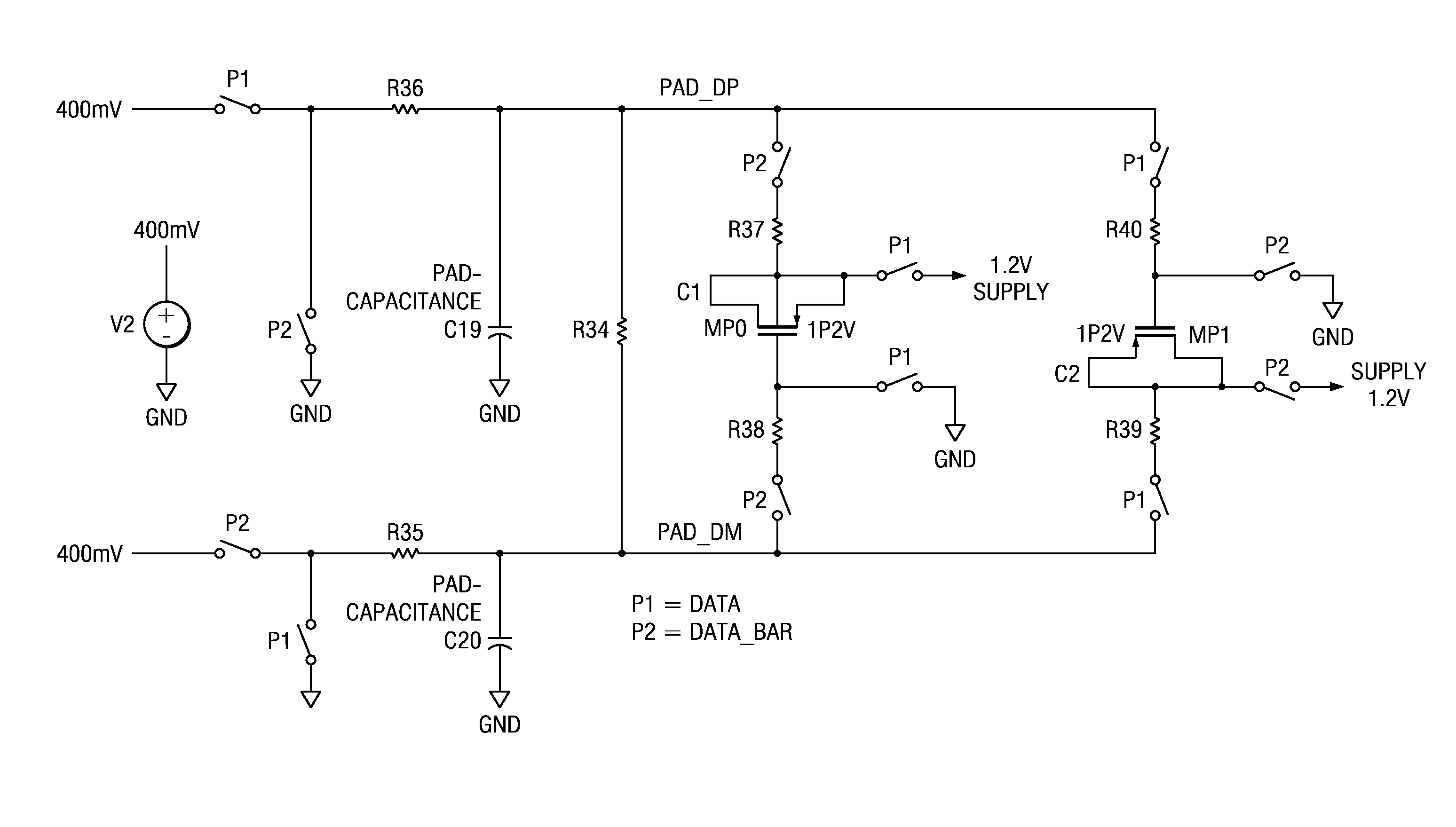
Effectively controls transition times without additional timing or current pulses, maintaining low common mode behavior and reducing high-frequency reflections, while being compact and economical, with minimal die-area overhead, improving rise and fall times from 70 ps to 245 ps in MIPI D-PHY compliant transmitters.

Problems solved by technology

Very fast transitions cause EMI (Electro Magnetic Interference) and very slow transitions result in poor receiver performance.
In such cases the rise / fall times become very small, and a method is required to increase the transition times. In some other applications, there might be too much pad capacitance on the pads, owing to high-capacitance ESD structures or the self-capacitance of other transmitters and receivers sharing the same pads.
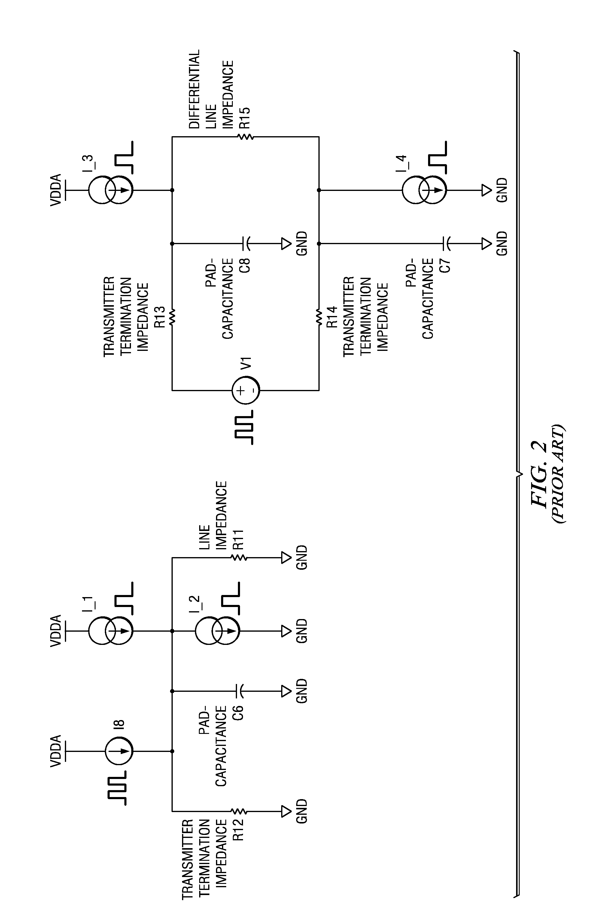
There are two disadvantages to the prior art scheme shown in FIG. 2.
This implies generating an accurate timing which is a small fraction of the data rate itself, which is a difficult and jitter-prone proposition at high data rates.
Second, for low voltage swing, low common mode applications (and these are becoming increasingly popular) the current sources which sink current (I_2 and I_4) will not have enough voltage headroom.
The scheme based on current pulses will be difficult to design.
Also, generating accurate pulses with width in 10 s of pico-seconds is a difficult and costly proposition.

Method used


Image

  • Scheme for controlling rise-fall times in signal transitions
  • Scheme for controlling rise-fall times in signal transitions
  • Scheme for controlling rise-fall times in signal transitions

Examples


Embodiment Construction

[0025]A detailed description of one or more embodiments of the invention is provided below in the context of the accompanying figures that illustrate by way of example the principles of the invention. While the invention is described in connection with such embodiments, it should be understood that the invention is not limited to any embodiment. On the contrary, the scope of the invention is limited only by the appended claims and the invention encompasses numerous alternatives, modifications and equivalents. For the purpose of example, numerous specific details are set forth in the following description in order to provide a thorough understanding of the present invention.

[0026]The present invention may be practiced according to the claims without some or all of these specific details. For the purpose of clarity, technical material that is known in the technical fields related to the invention has not been described in detail so that the crux of the present invention is not unneces...


PUM


Abstract

A serial interface interacting with a transmission pad system circuitry wherein a differential impedance is reckoned across the system voltage source, includes a scheme for controlling transmitter rise-fall transitions (to selectively speed up or slow down transitions) without requiring additional timing controls or affecting reflection coefficient of the transmitter port. The scheme uses at least one pre-charged capacitor, e.g., PMOS capacitor, interacting with the transmitter pad and connected through resistances or otherwise across the differential impedance with a switch. A modified scheme uses first and second parallely connected PMOS capacitors connectable with the transmission pad by switches, which may be NMOS switches. The scheme may be used in a MIPI D-PHY compliant DSI transmitter operating at, for e.g. 800 Mbps, and low signal common-modes. The scheme controls signal transition times of high speed circuitry including transmitters and uses a DATA signal which is already available to the circuitry.

Description

FIELD OF THE INVENTION[0001]This invention relates generally to improvements in the design of high speed signal circuitry such as for example, serial interfaces, and more particularly to a scheme for controlling the rise and fall times of the signal transitions in circuitry such as in serial interfaces.BACKGROUND OF THE INVENTION[0002]In high speed signal circuitry such as transmitters which might be used with serial interfaces, it is desirable to have controlled rise / fall times for output transitions. Very fast transitions cause EMI (Electro Magnetic Interference) and very slow transitions result in poor receiver performance.[0003]The rise and fall times at the transmitter pad are determined by: the output impedance of the driver, the characteristic impedance of the transmission line and the total lumped capacitance on the pad. The rise and fall times can be represented by simple RC charge and discharge. (Herein, the word capacitance is written abbreviated sometimes as “cap”).[0004...

Claims


Application Information

Patent Timeline
Patent Type & Authority Patents(United States)
IPC IPC(8): H03K5/12
CPCH03K19/0005H03K19/00361H04L25/12H04L25/0282H04L25/0288H04L25/0276H04L25/0278
Inventor KAMATH, ANANT SHANKAR
Owner TEXAS INSTR INC
Learn More