Active CMOS biosensor chip for fluorescent-based detection

a biosensor and fluorescent-based technology, applied in the field of fluorescent-based detection, can solve the problems of high detection limit, high optical filter requirements, complex instruments, etc., and achieve the effect of facilitating optical filter requirements, detailed characterization of fluorophore labels and their environmen

Active Publication Date: 2010-06-15
THE TRUSTEES OF COLUMBIA UNIV IN THE CITY OF NEW YORK
View PDF26 Cites 94 Cited by
  • Summary
  • Abstract
  • Description
  • Claims
  • Application Information

AI Technical Summary

Benefits of technology

[0018]In addition to its low-cost, compact form, the biosensor chip provides capabilities beyond those of macroscopic instrumentation by enabling time-gated operation for background rejection, easing requirements on optical filters, and by characterizing fluorescence lifetime, allowing for a more detailed characterization of fluorophore labels and their environment. The biosensor chip can be used for a variety of applications including biological, medical, and in-the-field applications. The biosensor chip can be used for DNA and protein microarrays where the biomolecular probe is attached directly to the chip surface. The biosensor chip can also be used as a general fluorescent lifetime imager in a wide-field or confocal microscopy system. For example, the biosensor chip can be used as an imager in a conventional widefield epifluorescent microscope for lifetime imaging.

Problems solved by technology

Actual detection limits are usually several orders of magnitude greater than this and are limited by background—either the effectiveness of optical filtering in removing the excitation wavelength or in removing stray fluorescence.
Lower excitation power also results in higher detection limits.
Such instruments are often expensive, large, and complex.

Method used


Image

  • Active CMOS biosensor chip for fluorescent-based detection
  • Active CMOS biosensor chip for fluorescent-based detection
  • Active CMOS biosensor chip for fluorescent-based detection

Examples


Embodiment Construction

[0045]In the following description, numerous specific details are set forth regarding the systems and methods of the present invention and the environment in which such systems and methods may operate, etc., in order to provide a thorough understanding of the present invention. It will be apparent to one skilled in the art, however, that the present invention may be practiced without such specific details, and that certain features, which are well known in the art, are not described in detail in order to avoid complication of the subject matter of the present invention. In addition, it will be understood that the examples provided below are exemplary, and that it is contemplated that there are other systems and methods that are within the scope of the present invention.

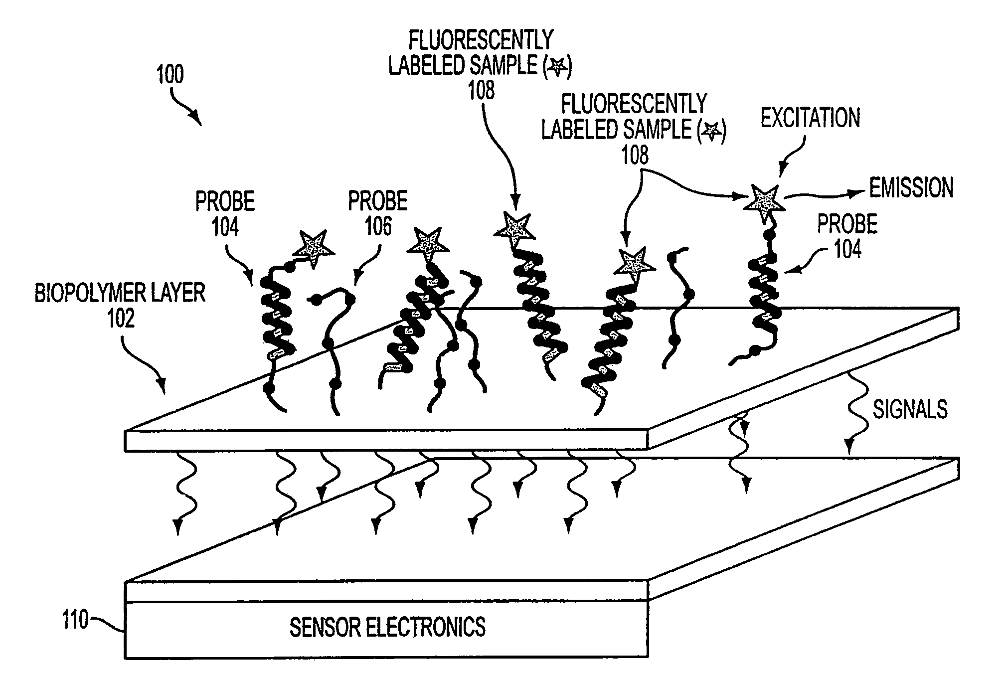
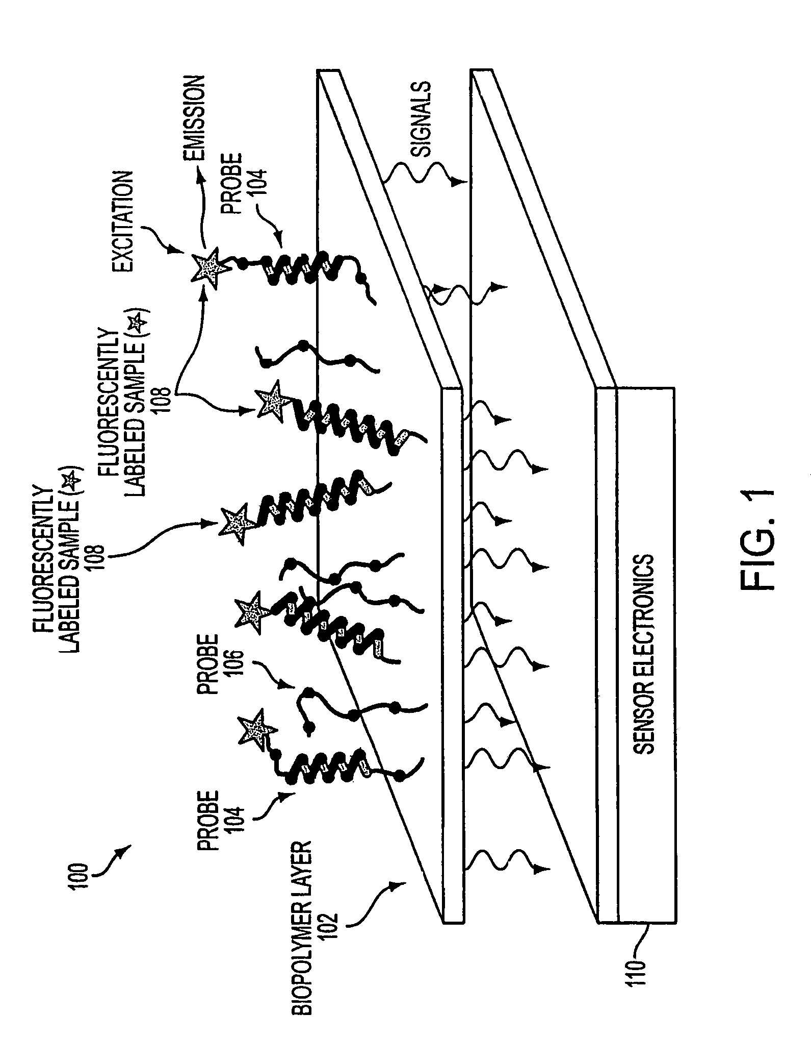
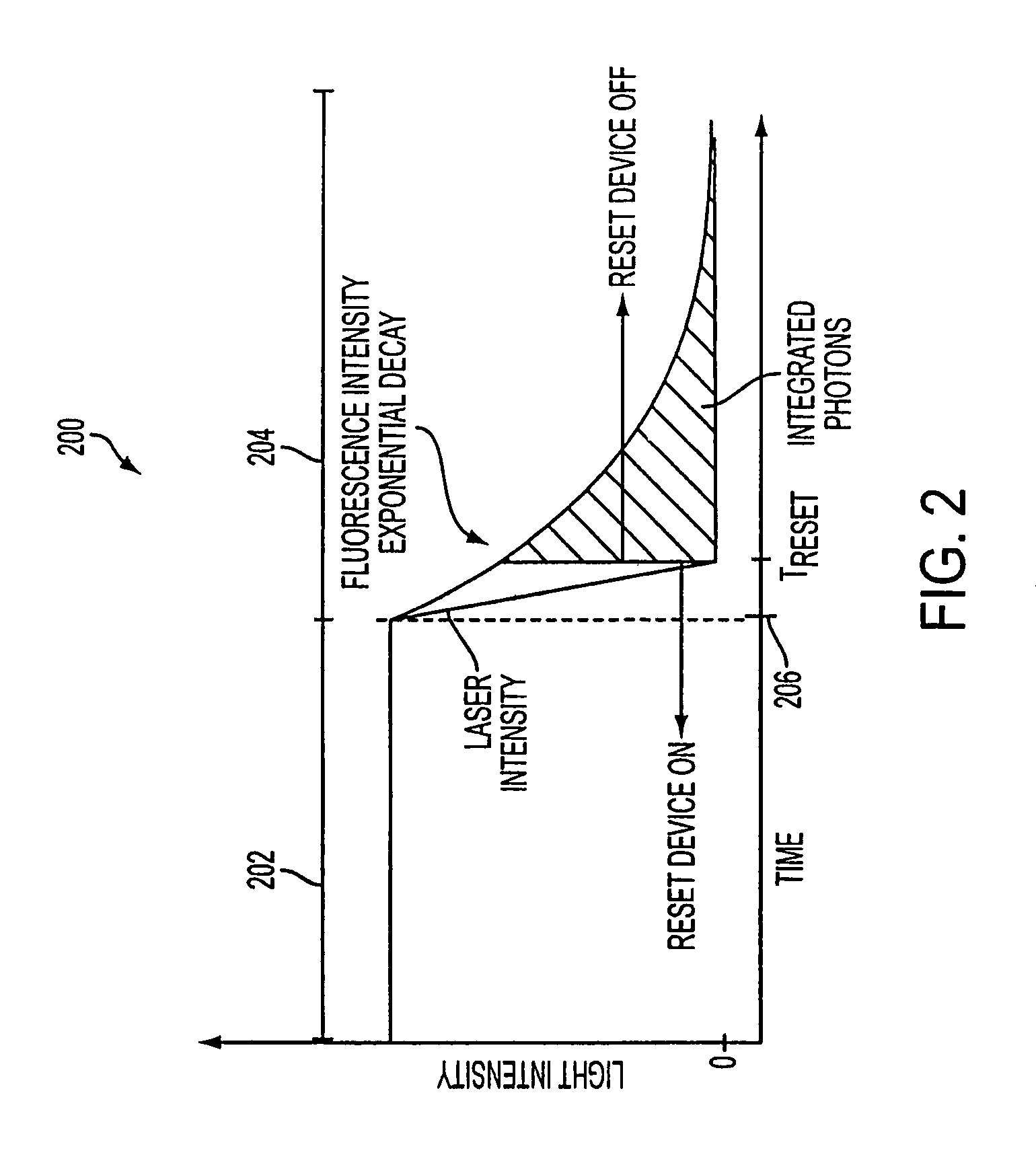
[0046]In accordance with the present invention, an active complementary metal oxide semiconductor (CMOS) biosensor chip is provided for fluorescent-based detection. The present invention provides several advantages. T...


PUM

PropertyMeasurementUnit
peak quantum efficiencyaaaaaaaaaa
resistanceaaaaaaaaaa

Abstract

An active CMOS biosensor chip for fluorescent-based detection is provided that enables time-gated, time-resolved fluorescence spectroscopy. In one embodiment, analytes are loaded with fluorophores that are bound to probe molecules immobilized on the surface of the chip. Photodiodes and other circuitry in the chip are used to measure the fluorescent intensity of the fluorophore at different times. These measurements are then averaged to generate a representation of the transient fluorescent decay response unique to the fluorophores. In addition to its low-cost, compact form, the biosensor chip provides capabilities beyond those of macroscopic instrumentation by enabling time-gated operation for background rejection, easing requirements on optical filters, and by characterizing fluorescence lifetime, allowing for a more detailed characterization of fluorophore labels and their environment. The biosensor chip can be used for a variety of applications including biological, medical, in-the-field applications, and fluorescent lifetime imaging applications.

Description

CROSS-REFERENCE TO RELATED APPLICATION[0001]This application is a continuation-in-part of U.S. patent application Ser. No. 11 / 431,405, filed May 9, 2006, which claims the benefit under 35 U.S.C. §119(e) of U.S. Provisional Patent Application No. 60 / 679,545, filed May 9, 2005, which are hereby incorporated by reference herein in its entirety. This application also claims the benefit under 35 U.S.C. §119(e) of U.S. Provisional Patent Application No. 60 / 799,408, filed May 9, 2006, which is hereby incorporated by reference herein in its entirety.STATEMENT REGARDING FEDERALLY SPONSORED RESEARCH[0002]This invention was made with United States Government support under National Science Foundation Grant No. BES-0428544 and National Institutes of Health Grant No. HG003089. The United States Government may have certain rights in this invention.BACKGROUND OF THE INVENTION[0003]1. Technical Field[0004]The present invention relates to fluorescent-based detection. More particularly, the present in...

Claims


Application Information

Patent Timeline
Patent Type & Authority Patents(United States)
IPC IPC(8): G01N21/00
CPCG01N21/6408G01N21/6428G01N21/6454H04N5/37452H04N3/155H01L27/14643H01L27/14621H04N25/771
Inventor SHEPARD, KENNETH L.LEVICKY, RASTISLAVPATOUNAKIS, GEORGE
Owner THE TRUSTEES OF COLUMBIA UNIV IN THE CITY OF NEW YORK
Why Eureka
Try Eureka