Method and mechanism for implementing electronic designs having power information specifications background

a technology of power information and design background, applied in the direction of cad circuit design, program control, instruments, etc., can solve the problems of increasing the difficulty of power management of such devices, unable to capture the intended behavior in the rtl, and increasing the difficulty of power management, so as to achieve low power design

Active Publication Date: 2010-06-15
CADENCE DESIGN SYST INC
View PDF29 Cites 39 Cited by
  • Summary
  • Abstract
  • Description
  • Claims
  • Application Information

AI Technical Summary

Problems solved by technology

This has resulted in more and more functionality being incorporated into battery-operated products, increasing challenges for power management of such devices.
These challenges are expected to become even more difficult with the continuous shrinking of process nodes using today's CMOS technology.
These advanced power management design techniques significantly change the design intent, yet none of the intended behavior can be captured in the RTL.
This creates a large gap in the RTL to GDSII implementation and verification flow where the original RTL is no longer reliable and cannot be used to verify the final netlist implementation containing the advanced power management techniques.
In addition, these specialized power management techniques at the physical implementation stage cannot be used by EDA tools at other stages of the design process, and therefore cannot be used by EDA tools at an earlier RTL or gate level stage of the IC design process to perform, for example, functional verification.
One reason this is important is because verification of low power designs only at the physical implementation stage of the design process may not capture all potential design flaws within the IC, particularly sequence-related problems for power modes that are ideally tested at the functional stage of the IC design process.

Method used


Image

  • Method and mechanism for implementing electronic designs having power information specifications background
  • Method and mechanism for implementing electronic designs having power information specifications background
  • Method and mechanism for implementing electronic designs having power information specifications background

Examples


Embodiment Construction

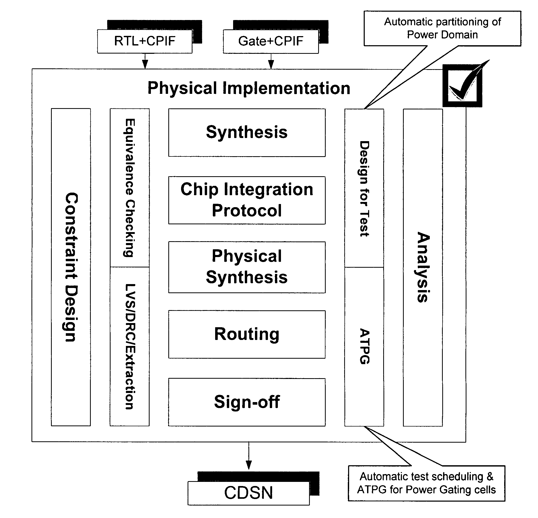
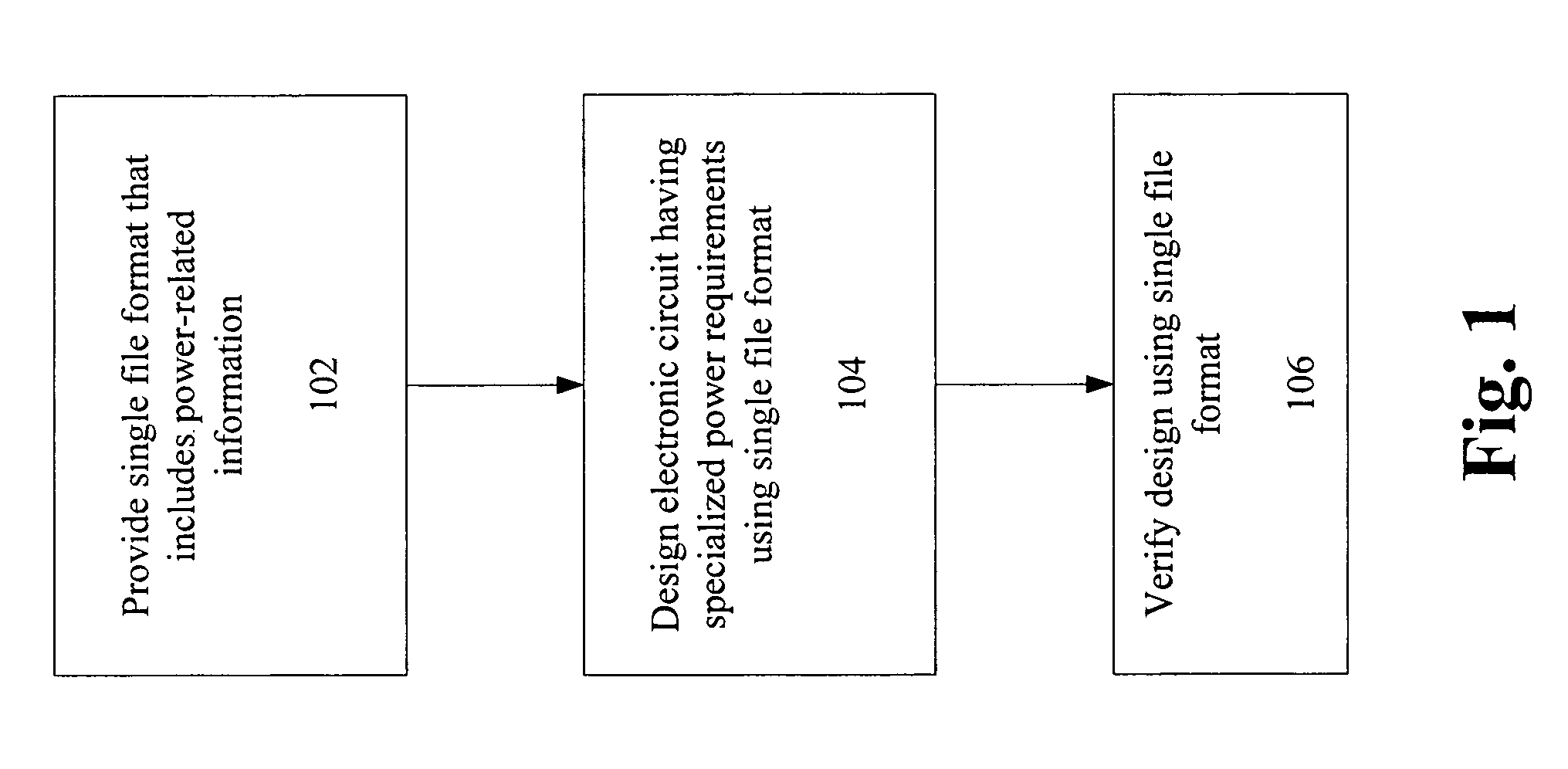
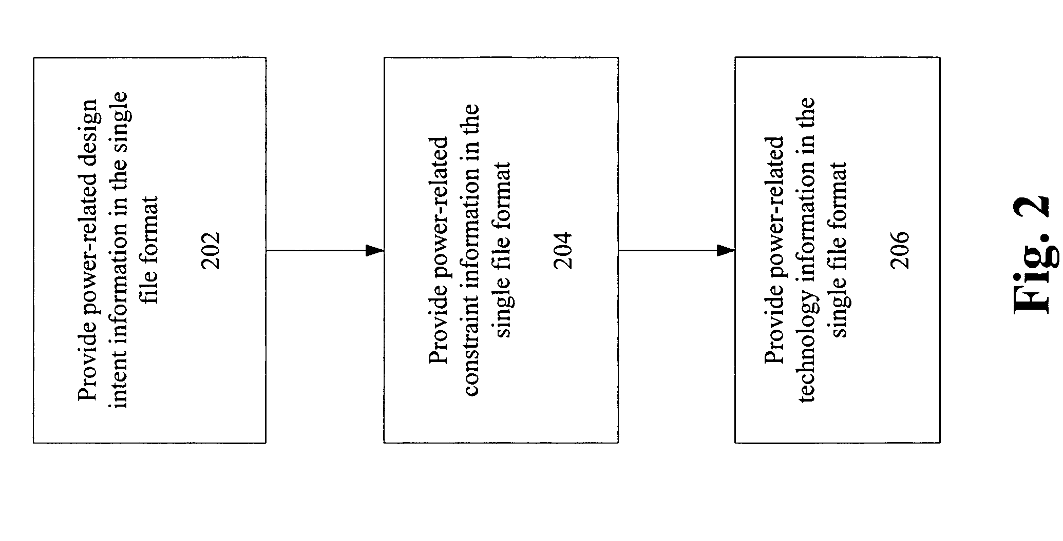
[0025]Some embodiments of the present invention provide an improved method and system for implementing electronic circuits with specialized power requirements, such as low power designs. As used herein, the term “implementing electronic circuits” includes at least activities for design creation, verification, physical implementation, analysis, and sign-off of the electronic design.

[0026]As noted above, many modern IC designs have special power requirements that are important for the proper operation of the IC's final electronic product. For example, consider a mobile or cellular telephone product. Such products are designed for portable use, and hence any ICs that are intended for use in cellular telephones may need to be designed with special power management requirements to prolong battery life. Therefore, ICs that are intended for mobile products such as cellular telephones are often designed with low power requirements and specifications.

[0027]In some embodiments, the invention ...


PUM


Abstract

A method of adding power control circuitry to a circuit design at each of an RTL and a netlist level comprising: demarcating multiple power domains within the circuit design; specifying multiple power modes each power mode corresponding to a different combination of on / off states of the multiple demarcated power domains; and defining isolation behavior relative to respective power domains.

Description

CROSS REFERENCE TO RELATED APPLICATIONS[0001]This patent application claims priority to U.S. Provisional Patent Application Ser. No. 60 / 792,060, filed Apr. 14, 2006, which is expressly incorporated herein by this reference.[0002]The following commonly owned patent applications as follows were filed on the dates indicated: U.S. Ser. No. 11 / 447,683 filed Jun. 5, 2006 entitled OPTIMIZED MAPPING OF AN INTEGRATED CIRCUIT DESIGN TO MULTIPLE CELL LIBRARIES DURING A SINGLE SYNTHESIS PASS, now U.S. Pat. No. 7,530,047; U.S. Ser. No. 11 / 489,384 filed Jul. 18, 2006 entitled METHOD AND SYSTEM FOR SIMULATING STATE RETENTION OF AN RTL DESIGN, now U.S. Pat. No. 7,610,571; U.S. Ser. No. 11 / 489,385 filed Jul. 18, 2006 entitled SIMULATION OF POWER DOMAIN ISOLATION , now U.S. Pat. No. 7,596,769; U.S. Ser. No. 11 / 518,339 filed Sep. 8, 2006 entitled LOW POWER SCAN TEST FOR INTEGRATED CIRCUITS; U.S. Ser. No. 11 / 586,879 filed Oct. 25, 2006 entitled METHOD AND SYSTEM FOR EQUIVALENCE CHECKING OF A LOW POWER ...

Claims


Application Information

Patent Timeline
Patent Type & Authority Patents(United States)
IPC IPC(8): G06F17/50
CPCG06F17/505G06F17/5081G06F17/5022G06F2217/78G06F30/327G06F2119/06G06F30/398G06F30/33G06F30/3308
Inventor WANG, QIGUPTA, ANKURCHEN, PINHONGCHU, CHRISTINAPANDEY, MANISHTSAI, HUAN-CHIHBHATIA, SANDEEPCHEN, YONGHAOSHARP, STEVENCHICKERMANE, VIVEKGALLAGHER, PATRICK
Owner CADENCE DESIGN SYST INC
Why Eureka
Try Eureka