Image sensor and digital camera

a digital camera and image sensor technology, applied in the field of image sensor and digital camera, can solve the problems of insufficient effect of improving moiré through optical low-pass filter, and deteriorating the quality of a photographed image, so as to achieve high-sensitivity, high-resolution, and suppress the effect of occurren

Inactive Publication Date: 2010-06-22
FUJIFILM CORP
View PDF27 Cites 30 Cited by
  • Summary
  • Abstract
  • Description
  • Claims
  • Application Information

AI Technical Summary

Benefits of technology

[0030]The invention aims for providing an inexpensive color solid-state image pickup device of single chip type which suppresses occurrence of a false signal (aliasing or Moiré and a false color and enables high-sensitivity, high-resolution, and faithful color reproduction.

Problems solved by technology

(1) When an image having a spatial frequency higher than the Nyquist frequency determined by a pitch between the photodiodes is projected on a color solid-state image pickup device, the high spatial frequency component is folded toward a low-frequency range, thereby resulting in generation of a false signal called aliasing or a Moiré and deteriorating the quality of a photographed image.
Consequently, a phenomenon called a false color or a color Moiré is induced, thereby deteriorating the quality of the photographed image.
However, the effect of improving Moiré by use of the optical low-pass filter is insufficient.
A structure in which an optical low-pass filter is attached to a package for protecting an image sensor suffers a problem of a hike in manufacturing costs as well as a problem of the optical low-pass filter being likely to be broken by mechanical stress inflicted on the package.
However, in order to integrate a plurality of photodiodes such as millions of pixels on one chip, other problems have come up as follows.
Formation of another lens makes the structure of the microlens complicated, thereby posing difficulty in achieving stable manufacturing yield.
Even if an image of a bright object is captured, a problem of insufficient sensitivity will arise.
Laying all the wiring electrodes within a single plane while preventing electrical contact is not possible.
Hence, adoption of the improvement means (1), (2) has been difficult.
As a result, there arises a problem of a relative decrease arising in the area of the light-receiving section of the photodiode.
Moreover, there also arises a problem of a necessity for laying multilayer metal wiring on the surface of the image pickup element in the X and Y directions.

Method used


Image

  • Image sensor and digital camera
  • Image sensor and digital camera
  • Image sensor and digital camera

Examples


first embodiment

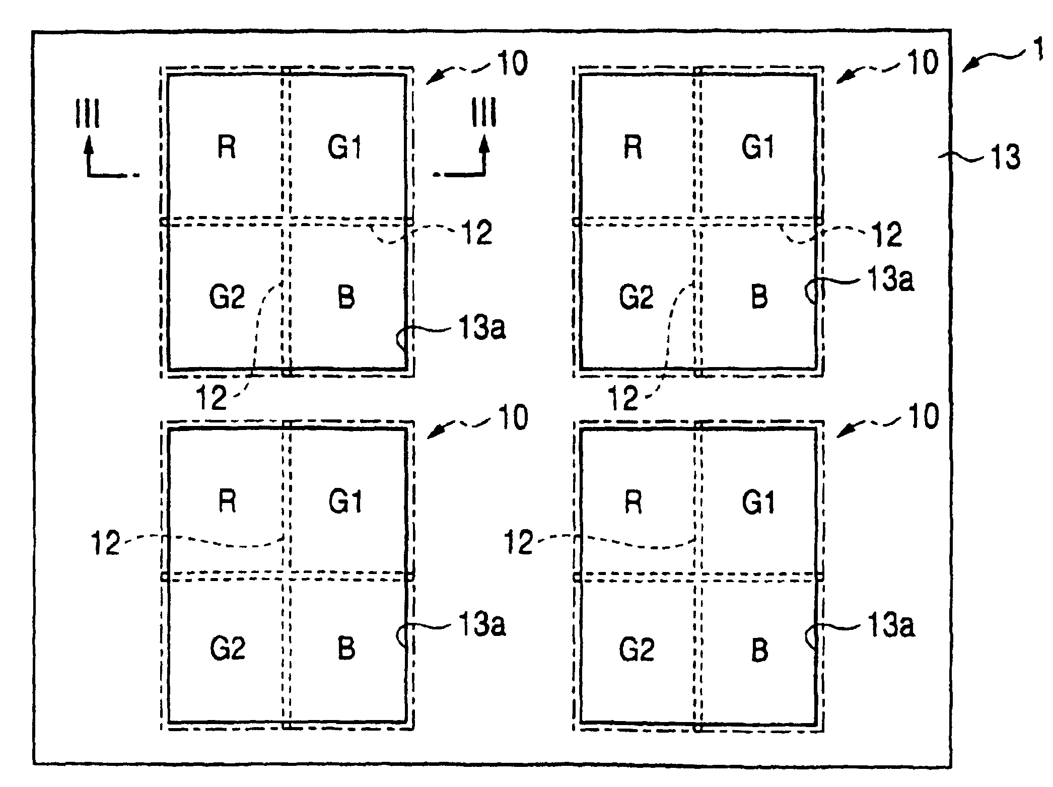
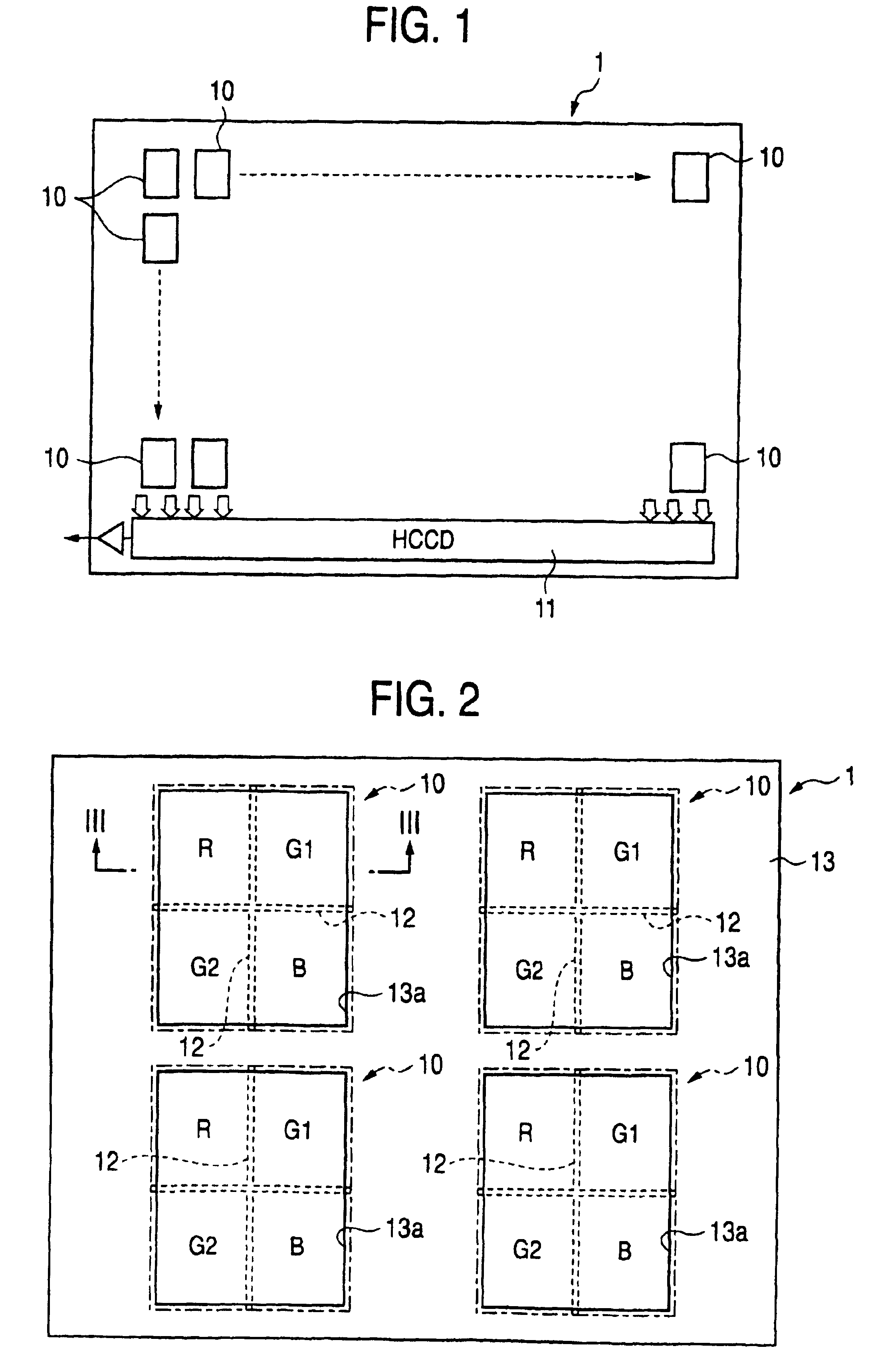
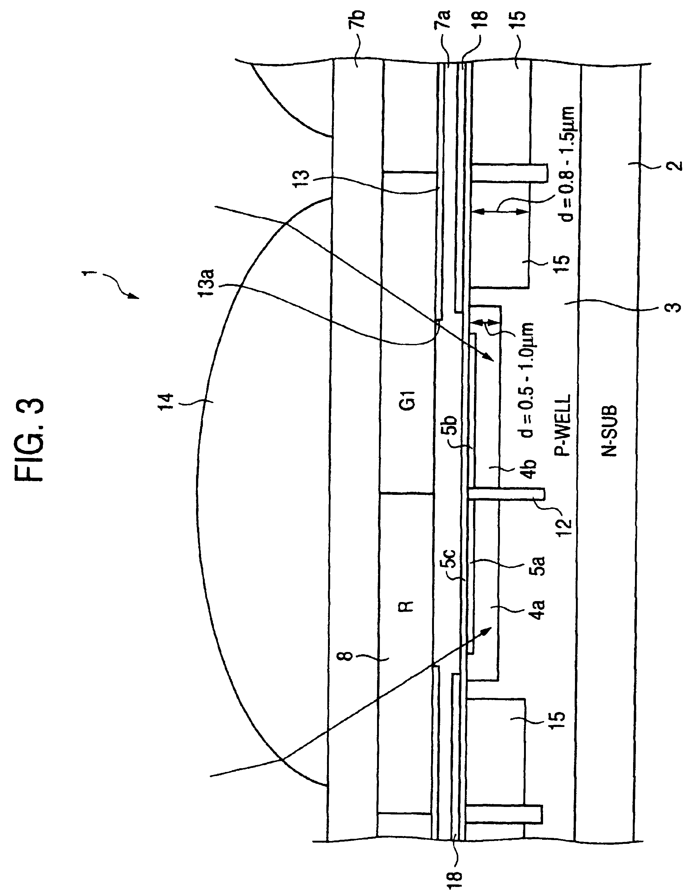
[0152]FIG. 1 is a block diagram of a color solid-state image pickup device of single chip type according to a first embodiment of the invention. In this embodiment, photoelectric conversion regions 10 to be described in detail later (individual photoelectric conversion regions will hereinafter be called pixel sections) are provided and formed, in a square grid pattern, on the surface of the semiconductor substrate constituting the solid-state image pickup device 1 of single chip type of the embodiment.

[0153]The inside of each pixel section 10 is two-dimensionally partitioned into a plurality of segments having a plurality of different spectral sensitivities (the segments will also be called “small pixels”). Electric charges stored in the respective small pixels are sequentially read into a vertical transfer channel, the channel being formed so as to vertically pass through the pixels sections 10 adjoining each other in the horizontal direction shown in FIG. 1. The electric charges t...

second embodiment

[0168]FIG. 6 is an enlarged plan view of the principal section of a color solid-state image pickup device according to a second embodiment of the invention, showing four pixel sections provided with the light-shielding film. In the first embodiment, the small pixels; that is, the small pixels R, G1, G2, and B, are arranged in the same pattern within all the pixel sections 10. However, in this embodiment, the arrangement of the small pixels R, G1, G2, and B is regularly changed from one pixel section to another pixel section. This is intended for diminishing a cyclic false signal stemming from the arrangement of a color filter.

[0169]When the arrangement of small pixels having different spectral sensitivities is to be changed within the pixel section,

[0170](1) a conceivable measure is to alternately switch vertical and horizontal color layouts on a per-column or per-row basis in the pixel section; and

[0171](2) another conceivable measure is to change the arrangement of a color filter ...

third embodiment

[0173]FIG. 7 is an enlarged plan view of the principal section of a color solid-state image pickup device according to a third embodiment of the invention, showing four pixel sections provided with the light-shielding film. The first embodiment has used primary-color-based color filters, and two kinds of filters G1, G2 as green color filters. In contrast, the present embodiment employs complementary-color-based four color filters yellow (Ye), magenta (Mg), cyan (Cy), and green (G).

[0174]The complementary-color-based color filters are formed from four colors. When a pixel section is formed from four small pixels as in the case of the present embodiment, four colors are convenient for allocating the colors to the respective small pixels. Even in this embodiment, as in the case of the second embodiment, a cyclic change in the arrangement of the small pixels Ye, Cy, Mg, and G within each pixel section is preferable.


PUM


Abstract

A color solid-state image pickup device includes a plurality of photoelectric conversion areas provided in an array pattern on a surface of a semiconductor substrate. The inside of each of photoelectric conversion areas 10 is two-dimensionally partitioned into a plurality of segments R, G1, G2, and B which output a plurality of photoelectric conversion signals of different spectral sensitivities. As a result, occurrence of a false signal and a false color is suppressed, and high-sensitivity, high-resolution image data having superior color reproducibility can be obtained.

Description

[0001]This nonprovisional application claims priority under 35 U.S.C. §119(a) on Patent Application No. 2002-335193 filed in JAPAN on Nov. 19, 2002 and Patent Application No. 2002-349921 filed in JAPAN on Dec. 2, 2002, the entire contents of which are hereby incorporated by reference.BACKGROUND OF THE INVENTION[0002]1. Field of the Invention[0003]The invention relates to a color solid-state image pickup device of single chip type and to a digital camera equipped with the color solid-state image pickup device.[0004]2. Description of the Related Art[0005]A typical color representation means employed in a solid-state image pickup device such as a CCD or CMOS types consisting of color representation means (i.e., a color solid-state image pickup device of single chip type) in which micro-color filters having three or four different spectral characteristics are arranged, in a mosaic pattern, on respective photodiodes (pixels) arranged on the surface of an image pickup element in the form ...

Claims


Application Information

Patent Timeline
Patent Type & Authority Patents(United States)
IPC IPC(8): H04N3/14H04N9/07H04N9/04
CPCH04N9/045H01L27/14627H01L27/14647H01L27/14623H04N23/84H04N25/134
Inventor SHIZUKUISHI, MAKOTO
Owner FUJIFILM CORP
Why Eureka
Try Eureka