Tilted combiners/decombiners and photonic integrated circuits (PICs) employing the same

a technology of combiners/decombiners and integrated circuits, applied in the field of combiners/decombiners, can solve the problem that no longer can be deployed as optical inputs to combiners, and achieve the effect of less power, more power, and thermal budg

Inactive Publication Date: 2010-06-29
INFINERA CORP
View PDF158 Cites 11 Cited by
  • Summary
  • Abstract
  • Description
  • Claims
  • Application Information

AI Technical Summary

Benefits of technology

[0023]According to this invention, a monolithic optical transmitter photonic integrated circuit (TxPIC) comprises a plurality of integrated modulated sources having an array of laser sources with power outputs, at constant current, varying across the array similar to a quadratic-shaped curve and, further, forming an array of signal channels each having a different wavelength output which are a series of regularly spaced wavelengths. An optical combiner / decombiner is integrated in the circuit and has at least one free space region to receive a plurality of waveguides each respectively carrying a signal wavelength output from a modulated source. The optical combiner / decombiner may be of the non-reflective or transmissive type or of the reflective type. The free space region has a plurality of ordered bands along its edge where the zero order band is substantially at a longitudinal centerline of the free space region where, on either side of this band, is a first order band followed by additional higher order bands. The ends of the output waveguides from the modulated sources may be coupled approximate to the free space region edge along a region of the zero order band between one of the adjacent first order bands and a longitudinal centerline of the zero order band so that the inputs of the signal channels to the combiner of are titled or offset with respect to the longitudinal centerline of the combiner free space region so the combined outputs from the optical combiner will be aligned along the slope of the quadric-shaped curve of the combiner output passband envelope. This combiner passband quadric-shaped curve is substantially matched to the quadric-shaped curve of the predetermined active region wavelength spectrum of the modulated sources in such a way that enhanced power uniformity is achieved in a natural way across the modulated source array outputs as produced in the combiner output.
[0024]We refer to these waveguide input ends as provide to the combiner free space region as “tilted” because, by placing input ends into the free space region offset from the free space longitudinal centerline, a small angle is imposed by the offset input and that angle is tilted with respect to the free space region zero order band centerline. The same tilt will be projected at the output venires or spares of either the same (in the case of a reflective-type) or different (in the case of non-reflective or transmissive type) free space region of the combiner. The provision of a plurality of output spares along and offset within the zero order Brillouin zone of the combiner free space region, from whence the combined modulated source signal output is directed, provides for selection of one such output that is optimum relative to having the highest power performance.
[0027]Thus, the following advantages are realized from the deployment of a tilted combiner / decombiner of this invention. First, in this offset approach, a more compact reflective-type combiner / decombiner can be employed where the free space region functions as an output of the combiner as well as an input of the combiner. The output is offset from the centerline within the zero order band and may be in close proximity to a second adjacent first order band, on the opposite side of the free space region centerline from the free space input regions. Second, in the deployment of a titled input combiner of either the reflective-type or non-reflective-type integrated with an array of modulated sources in a monolithic photonic integrated circuit (PIC) where semiconductor lasers are employed as such sources and for any reason have a near quadratically varying output power versus channel number at a constant current the tilted input to the optical combiner / decombiner provides for a more evenly distributed power level across the modulated signal outputs from the integrated array of modulated sources. By tilting the inputs to the optical combiner, the natural passband filtering effect of the optical combiner can be deployed to provide more power to the weaker power laser sources and less power to the stronger power laser sources, thereby providing a natural contribution toward power equalization across the laser source outputs present at the output of the photonic integrated circuit (PIC). With the adaptation of this pre-distorted output power spectrum from the combiner integrated in a PIC, a lower PIC power, and thermal budget is achieved because of less required dependence, or no dependence in some circumstances, for on-chip optical AVE channel elements. The required bias current levels to such AVEs are reduced and, correspondingly, the thermal budget of the PIC chip is reduced. Also, since the power budget is decreased via less AVE bias current, the application of this invention provides for a TxPIC that may have more channels and / or operate at higher baud rates.

Problems solved by technology

In other words, if one of the inputs to a conventional reflective-type selective wavelength combiner is employed as an output, it no longer can be deployed as an optical input to the combiner.

Method used


Image

  • Tilted combiners/decombiners and photonic integrated circuits (PICs) employing the same
  • Tilted combiners/decombiners and photonic integrated circuits (PICs) employing the same
  • Tilted combiners/decombiners and photonic integrated circuits (PICs) employing the same

Examples


second embodiment

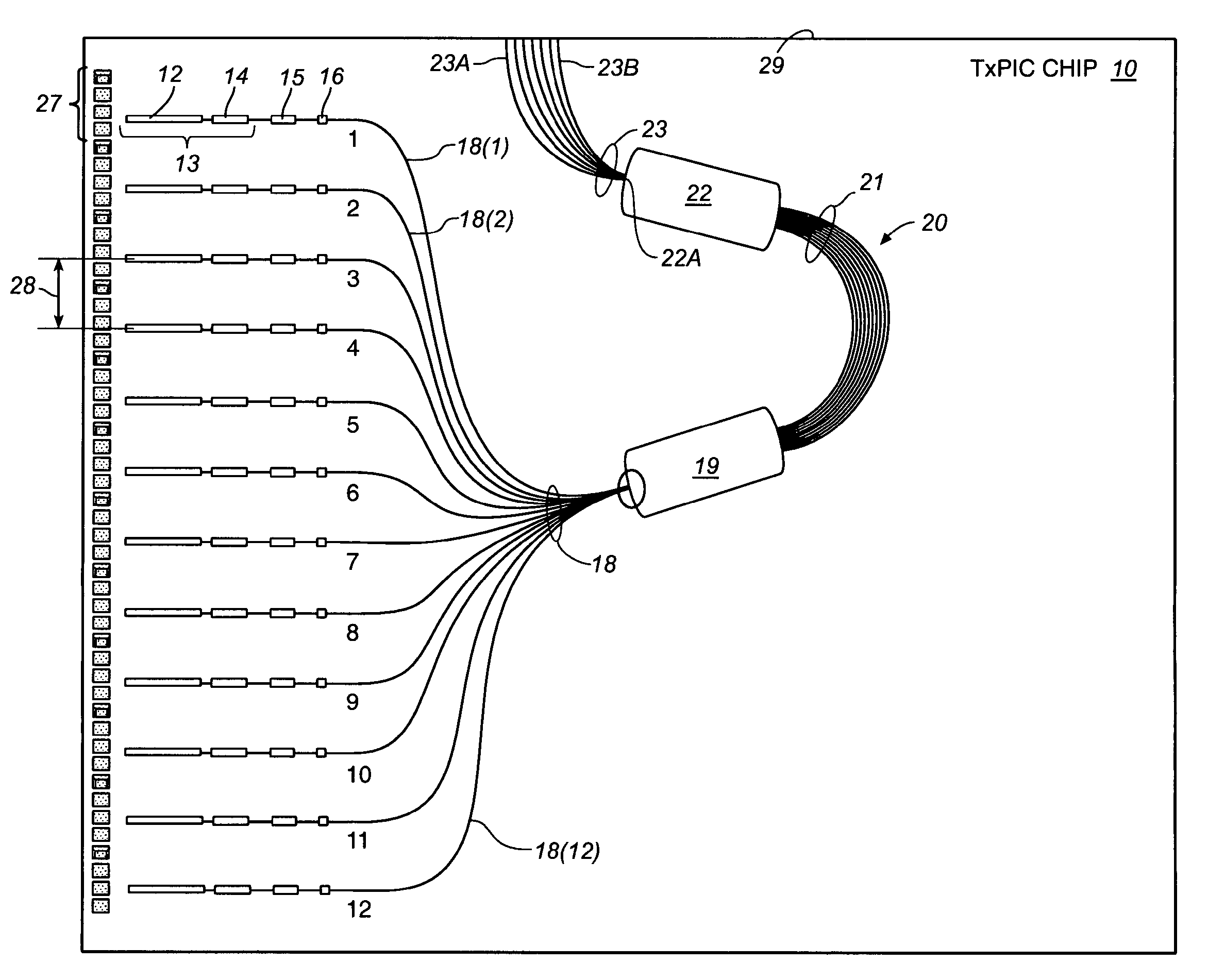
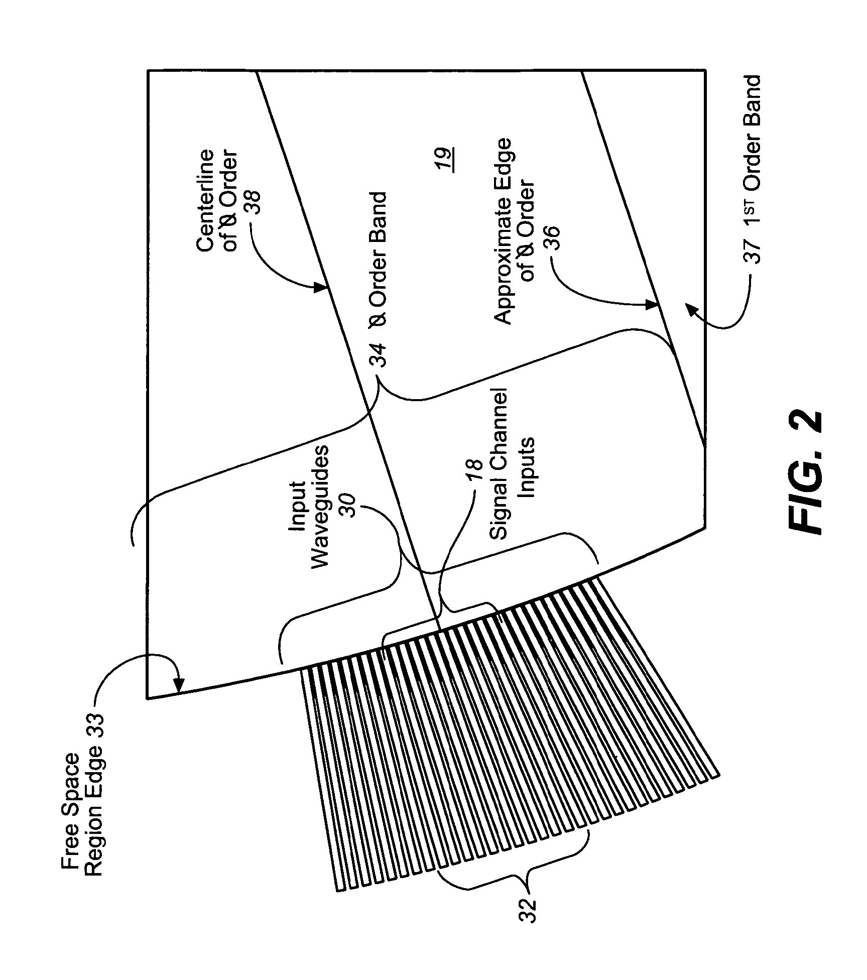
[0044]Reference is now made to this invention shown in FIGS. 6 and 7. TxPIC 60 in FIG. 6 comprises a plurality of integrated modulated sources 13 for providing channel signals on output waveguides 18 comprising channels Nos. 1-12. Each channel waveguide 18(1) . . . 18(12) is provided to an input / output free space region 64 of a reflective combiner 62 comprising, here, a reflective-type AWG. A reflective-type AWG is illustrated in the art as seen in U.S. Pat. No. 5,396,507 at device 7, which patent is incorporated herein by its reference. Reflective AWG 62 is optically the same as AWG 20 in FIG. 1 but physically different in construction in that the arrayed waveguide grating arms 63 approximate one-half the grating arms 21 of AWG 20 so that a single free space region 64 functions both as the input free space region 19 as well as output free space region 22 of AWG 20 of FIG. 1. A unique feature of reflective AWG 62 is that a portion 65 of grating arms 63 are substantially straight in ...


PUM


Abstract

A monolithic optical transmitter photonic integrated circuit (TxPIC) comprises a plurality of integrated modulated sources which, when all operated at constant current, display a power output that varies as a function of array position similar to a quadratic-shaped curve and, further, forming an array of signal channels each having a different wavelength output. An optical combiner / decombiner is integrated in the circuit and has at least one free space region with a plurality of ordered bands along its edge where the zero order band is substantially at a longitudinal centerline of the free space region and where, on either side of this band, is a first order band followed by additional higher order bands. The ends of the output waveguides from the modulated sources are coupled approximate to the free space region edge along a region of the zero order band between one of the adjacent first order bands and a longitudinal centerline of the zero order band so that the inputs of the signal channels to the combiner of are titled or offset with respect to the longitudinal centerline of the combiner free space region so the combined outputs from the optical combiner will be aligned along the slope of the quadric-shaped curve of the combiner output passband envelope. The tilted combiner / decombiner may also be deployed in a receiver photonic integrated circuit (RxPIC) or other circuit employing such a device.

Description

CROSS REFERENCE TO RELATED APPLICATIONS[0001]This application is a Divisional of application Ser. No. 11 / 377,155, filed Mar. 16, 2006, now U.S. Pat. No. 7,444,048 which claims priority of provisional application, Ser. No. 60 / 663,279, filed Mar. 18, 2005 and, further, is a continuation-in-part of patent application, Ser. No. 10 / 846,336, filed May 13, 2004 now U.S. Pat. No. 7,209,611 and entitled, TRANSMITTER AND RECEIVER PHOTONIC INTEGRATED CIRCUIT (TXPIC AND RXPIC) CHIPS UTILIZING COMPACT WAVELENGTH SELECTIVE COMBINERS / DECOMBINERS and published on Oct. 28, 2004 as Publication No. US 2004 / 0213582 A1, which claims priority to provisional application, Ser. No. 60 / 470,570, filed Apr. 14, 2003, which application is also incorporated herein by its reference, and is also a continuation-in-part of patent applications, Ser. No. 10 / 267,331, filed Oct. 8, 2002, now U.S. Pat. No. 7,283,694 also published on May 22, 2003 as Publication Ser. No. US 2003 / 0095737 A1, and entitled, TRANSMITTER PHOTO...

Claims


Application Information

Patent Timeline
Patent Type & Authority Patents(United States)
IPC IPC(8): G02B6/34G02B6/43G02B6/26
CPCG02B6/12011G02B6/12019G02B6/12016
Inventor PETERS, FRANK H.JOYNER, CHARLES H.MISSEY, MARK J.
Owner INFINERA CORP
Why Eureka
Try Eureka