
Ball grid array package layout supporting many voltage splits and flexible split locations

a technology of flexible split and package layout, applied in the field of chip packaging, can solve the problems of multiple input/output power voltages, unable to support main power voltages of devices, etc., and achieve the effect of reducing power plane editing and high flexibility

Active Publication Date: 2010-07-06
BELL SEMICON LLC
View PDF4 Cites 2 Cited by
  • Summary
  • Abstract
  • Description
  • Claims
  • Application Information

AI Technical Summary

Benefits of technology

"The present invention is about a new package design for a semiconductor device. The package has multiple layers and paths for power and input / output signals. The design allows for flexibility in the placement and quantity of power splits, reduces the need for editing power planes, and avoids moving ball contact pads when a split is applied. The technical effects of this design include supporting many input / output power voltage splits, flexible split locations, and high flexibility in the placement of voltage splits."

Problems solved by technology

The conventional approaches are not able to support a main power voltage and multiple input / output power voltages or have flexible placement of the input / output power voltages along the die edge.

Method used


Image

  • Ball grid array package layout supporting many voltage splits and flexible split locations
  • Ball grid array package layout supporting many voltage splits and flexible split locations
  • Ball grid array package layout supporting many voltage splits and flexible split locations

Examples


Embodiment Construction

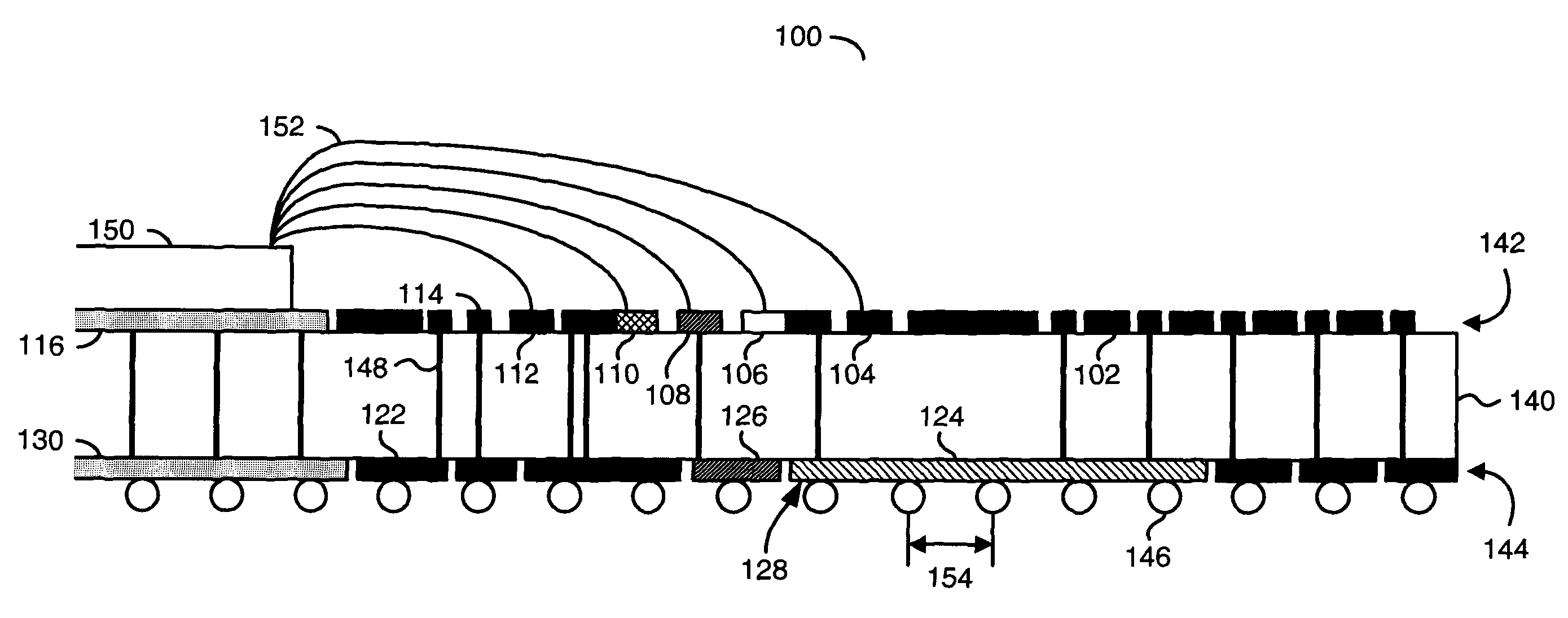
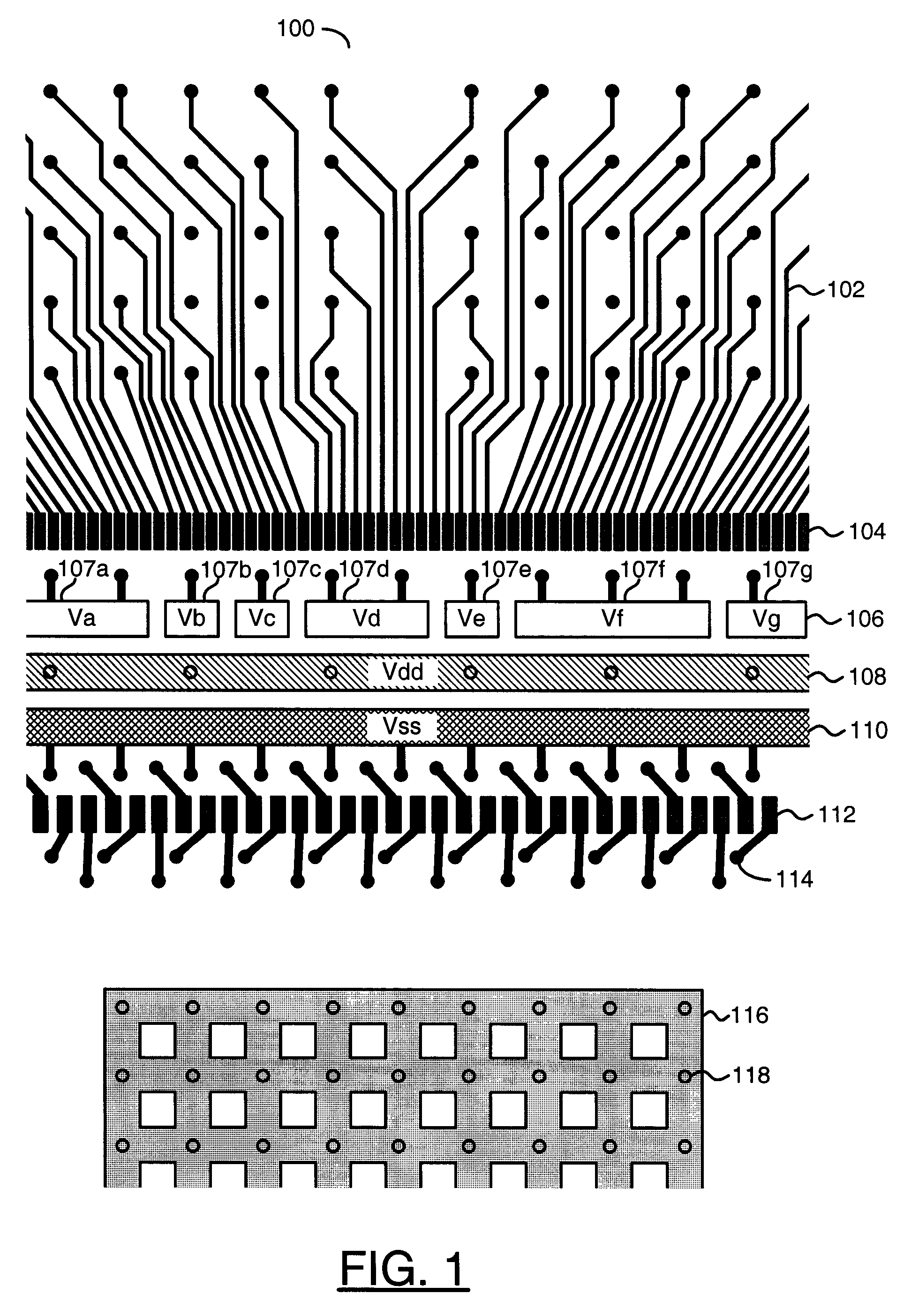
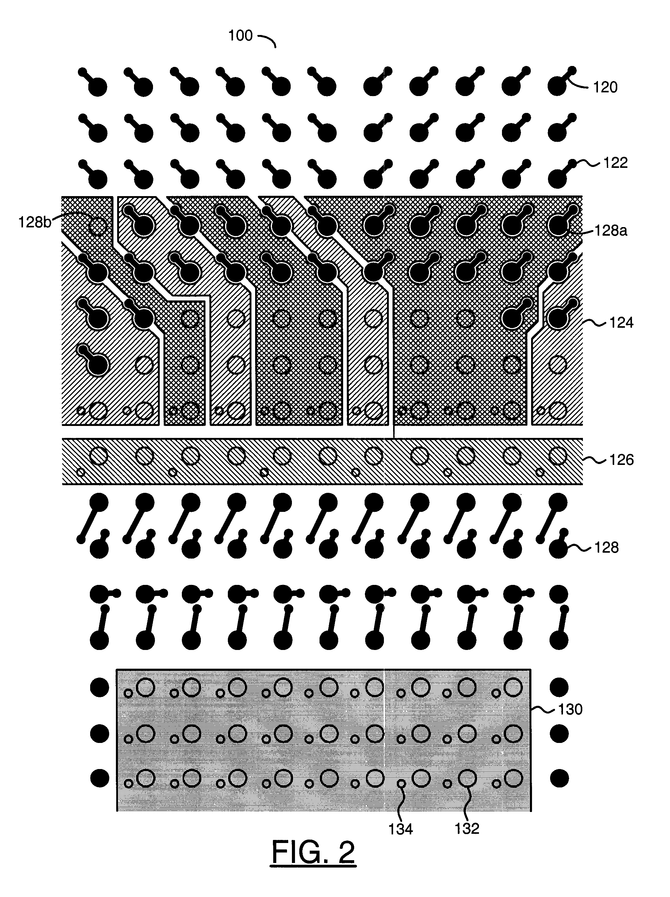
[0010]Contact pads (e.g., ball pads) that may bring power into a package are generally located directly below or nearby multiple voltage supply rings that may be located near a die (or chip) mounted on a substrate of the package. Solder balls (or pins) at each of the contact pads may be arranged in (i) a continuous array or (ii) a depopulated array. Vias generally interconnect the contact pads in a bottom conductive (e.g., metal) layer of the package up to the voltage supply rings in a top conductive (e.g., metal) layer of the package to form signal paths and power paths. For a package with a defined contact pitch, balls pitch or pin pitch (e.g., 1 millimeter), the present invention may support ring splits down to the contact pitch. Finer pitches may be achieved by using additional staggered rows of the contact pads. Other contact pitches, both coarser and finer, and / or arrangements may be implemented to meet the criteria of a particular application. Split power planes may be employ...


PUM


Abstract

A die package generally including (A) ground paths routing a power ground from a ground power set of contact pads in a first conductive layer to a ground ring in a second conductive layer, (B) core paths routing a core voltage from a core power set of contact pads in the first conductive layer to a core ring in the second conductive layer, and (C) input / output voltage paths routing input / output voltages from an input / output power set of contact pads in the first conductive layer to an input / output ring in the second conductive layer, (i) the input / output ring surrounding the core ring, (ii) the ring being configured to power input and output circuits of the die, (iii) the input / output ring being split into ring segments isolated from each other and (iv) at least one particular ring segment having a length of less than a single connector pitch.

Description

FIELD OF THE INVENTION[0001]The present invention relates to chip packaging generally and, more particularly, to a method and / or apparatus for implementing a Ball Grid Array (BGA) package layout supporting many voltage splits and flexible split locations.BACKGROUND OF THE INVENTION[0002]As integrated circuit package designs have evolved, an increasing interest has been created to supply multiple power voltages to the integrated circuit and have isolation in the power supply nets in the package. Conventional approaches of power distribution in the package support a ground ring and two different power voltage rings to power the integrated circuit. The conventional approaches are not able to support a main power voltage and multiple input / output power voltages or have flexible placement of the input / output power voltages along the die edge.SUMMARY OF THE INVENTION[0003]The present invention concerns a die package. The package generally comprises (A) a plurality of ground paths routing ...

Claims


Application Information

Patent Timeline
Patent Type & Authority Patents(United States)
IPC IPC(8): H01L23/52
CPCH01L23/49816H01L23/49838H01L23/50H01L24/49H01L23/49811H01L2224/48091H01L2224/48227H01L2224/49H01L2924/01005H01L2924/14H01L2924/1433H01L2924/15311H01L2924/15312H01L2924/3025H01L2924/00014H01L24/48H01L2924/01006H01L2924/01023H01L2924/01033H01L2924/014H01L2224/45099H01L2224/05599
Inventor FISHLEY, CLIFFORD R.AWUJOOLA, ABIOLAMORA, LEONARD L.
Owner BELL SEMICON LLC
Learn More