Image signal processing apparatus, image signal processing method and camera using the image signal processing apparatus

a signal processing and image signal technology, applied in the direction of color signal processing circuits, color television details, television systems, etc., can solve the problem the method cannot determine the shift the trouble of determining a normal pixel as a defective pixel, etc. problem, to achieve the effect of properly adjusting an offset value, high-quality image signal and increasing the circuit scal

Inactive Publication Date: 2010-07-06
CANON KK
View PDF13 Cites 12 Cited by
  • Summary
  • Abstract
  • Description
  • Claims
  • Application Information

AI Technical Summary

Benefits of technology

[0022]It is an object of the present invention to easily avoid that an image signal black-sinks by clamping float of an OB image output due to incoming of infrared light.
[0023]It is another object of the present invention to restrain the error of a clamp level even if a level shift occurs in a signal from a light shielded pixel without extremely increasing a circuit scale.
[0057]According to the present invention, it is possible to determine optical black float which is a smooth change of optical black pixel output according to infrared light ever horizontal line. Moreover, when detecting the optical black float, it is possible to prevent black sinkage which is a sinkage of an image in the black direction by a clamp operation by clamping an optical-black clamp operation by an already-held difference output and obtain a high-quality image signal.
[0058]According to the present invention, it is possible to remove a signal in which a level shift occurs or replace the signal with other signal even if a level shift occurs in some of signals from a plurality of light shielded pixels by a defect in a light shielded pixel in a solid state image sensor or incoming light by adding a few circuits. Therefore, the present invention makes it possible to properly adjust an offset value to be added to a signal from a solid state image sensor. Therefore, the present invention makes it possible to restrain that a clamp level error occurs without extremely increasing a circuit scale even if a level shift occurs in a signal from a light shielded pixel and apply preferable signal processing. Moreover, it is possible to allow a defect of a certain degree in the light shielded pixel portion of a solid state image sensor, moderate a selection reference and improve a yield.

Problems solved by technology

However, in the case of an OB pixel output shift smaller than 10 LSB, even the defect pixel determination method cannot determine the shift as a defective pixel.
Because a change of OB pixel outputs is smooth, the defect pixel determination method cannot determine the change.
However, this method causes a trouble of determining a normal pixel as a defective pixel due to noise when setting a determination level to 2 LSB.
However, many storage memories are required.
However, when setting the gain of the clamp circuit 156 to a small value, the following problem occurs.
That is, when shading in which an offset value changes in the vertical direction of a solid state image sensor is large, correction becomes insufficient.
Therefore, because a gain is actually set in accordance with the relation of the trade-off, sufficiently decreasing the gain value of the clamp circuit 156 is not sufficient to solve the above described problem.
However, this method has a problem that a circuit scale is increased because storing means is necessary, it is necessary to perform test and adjustment every solid state image sensor and an integrated circuit of a special process like a nonvolatile memory is necessary.
However, when the shift of a level of a signal from a light shielded pixel is large, there is a problem that it is impossible to sufficiently reduce errors at a clamp level though it is possible to reduce influences to a certain extent by averaging.

Method used


Image

  • Image signal processing apparatus, image signal processing method and camera using the image signal processing apparatus
  • Image signal processing apparatus, image signal processing method and camera using the image signal processing apparatus
  • Image signal processing apparatus, image signal processing method and camera using the image signal processing apparatus

Examples


first embodiment

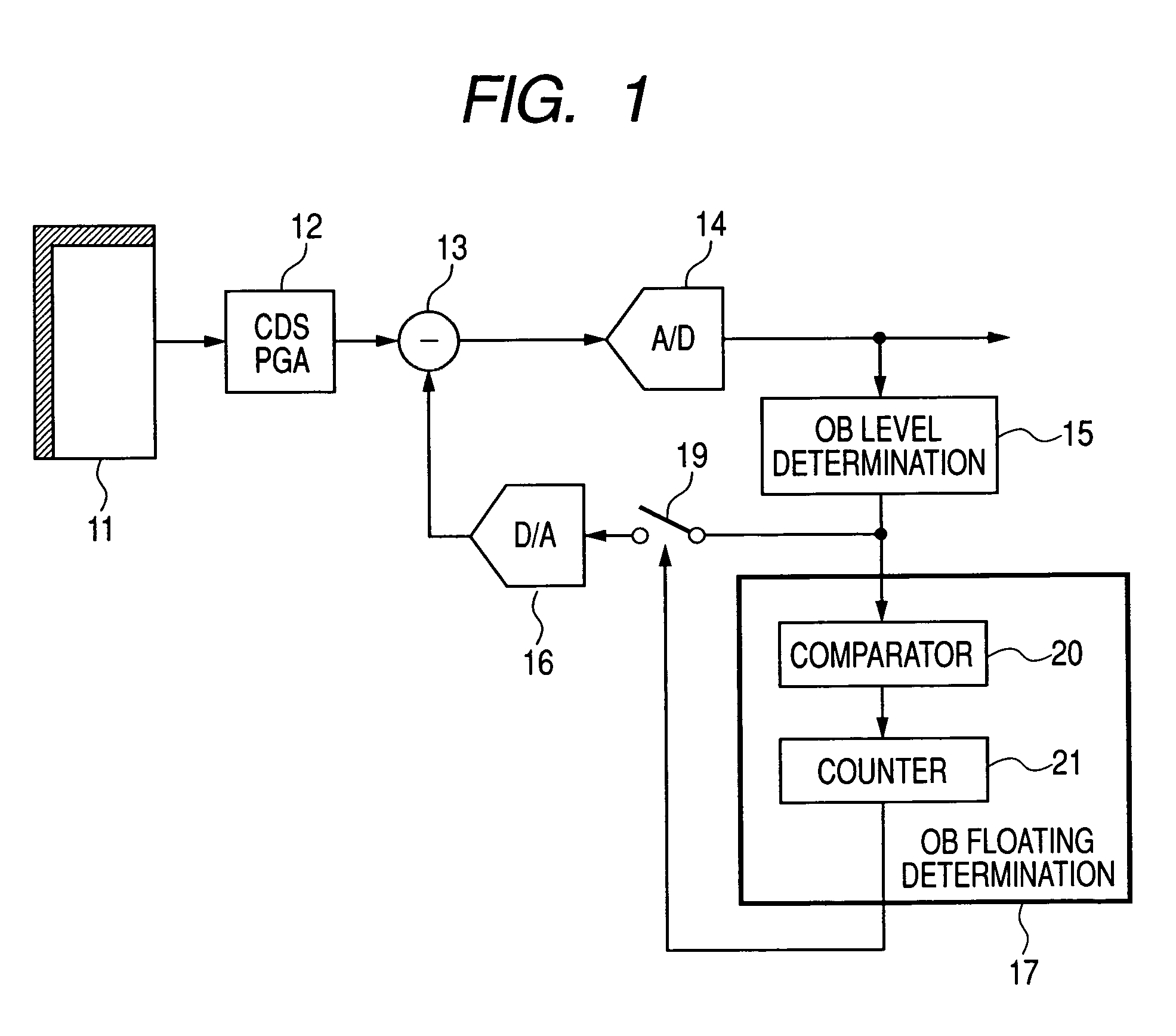
[0075]First embodiment of the present invention is described below in detail by referring to FIG. 1. In FIG. 1, reference numeral 11 denotes a CMOS sensor serving as a solid state image sensor such as a CCD. Reference numeral 12 denotes an analog signal processing block for first receiving an image signal from the solid state image sensor 11, which is mainly constituted of a CDS circuit for double-sampling a signal from the solid state image sensor 11 and a programmable gain control circuit (PGA circuit) for adjusting the amplitude level of a signal. An output of the analog signal processing block 12 is input to the adding and subtracting circuit 13 for adjusting an OB (optical black; hereafter referred to as OB) level and then, input to the A / D converter 14 for converting the output into a digital value.

[0076]The signal converted into a digital value is output to the outside and also input to a feedback loop. The feedback loop first compares an OB level converted by the A / D convert...

second embodiment

[0085]Second embodiment of the present invention is described below by referring to FIG. 3. In the case of the first embodiment, an example is shown in which clamp determination at a digital value after A / D conversion is fed back to an analog signal before A / D conversion. However, the clamp determination can be also applied to digital clamp immediately after controlling an output digital value, which is shown in FIG. 3 for description. Description of an object same as that in the first embodiment is omitted.

[0086]In FIG. 3, reference numeral 11 denotes a solid state image sensor and 12 denotes an analog signal processing block for first receiving an image signal from the solid state image sensor. An output of the analog signal processing block 12 is input to the A / D converter 14 for converting the output into a digital value. The signal converted into the digital value is input to an adder and subtractor 13 for clamp and moreover input to the OB determination block 15 to compare an ...

third embodiment

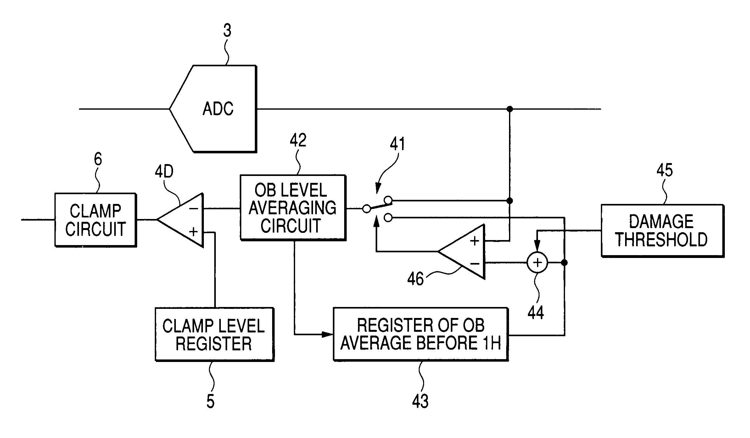
[0089]FIG. 4 is a block diagram showing a circuit configuration of an image signal processing apparatus of third embodiment of the present invention. In FIG. 4, the same symbol is provided for a block having a function same as that of the block shown in FIG. 15.

[0090]In FIG. 4, reference numeral 43 denotes an AD converter for converting an analog signal into a digital signal (digital data). An image signal from a solid state image sensor (e.g. CCD or CMOS sensor) having a plurality of effective pixels and a plurality of light shielded pixels is input to the AD converter 43 through not-illustrated CDS circuit and programmable gain amplifier and the AD converter 43 converts the image signal into a digital signal (digital data) and outputs the signal.

[0091]Reference numeral 411 denotes a digital filter detects and eliminates a signal whose level is shifted (abnormal level) among signals from light-shielded pixels output from the AD converter 43. That is, the digital filter 411 eliminat...


PUM


Abstract

When clamping a signal from a solid state image sensor, float of an optical black pixel output due to incoming of infrared light avoids a malfunction of a clamp from occurring. When clamping a signal from the solid state image sensor, the difference between the optical black pixel output and a clamp target level is output as a difference output, the difference output is compared with a comparison level to integrate the number of times larger than the comparison level every horizontal line. When the number of times is equal to or more than a certain rate (⅔) from the number of optical black pixels on the horizontal line, an optical black float state is determined and clamping operation is performed in accordance with a held value immediately before.

Description

BACKGROUND OF THE INVENTION[0001]1. Field of the Invention[0002]The present invention relates to an image signal processing technique for an image signal such as an optical black level output from a solid state image sensor such as a CMOS sensor or CCD, particularly to the control technique of clamping means in image signal processing.[0003]2. Related Background Art[0004]In general, a solid state image sensor such as a CMOS sensor outputs an optical black (hereafter referred to as OB) from a light shielded pixel as the reference of a signal level. A circuit for processing the signal of a sensor clamps an OB level to a predetermined level and then, performs signal processing such as conversion of the level to a digital value. Normally, as shown in FIG. 12, several light-shielded pixels for respectively outputting an OB level to be clamped are set to several horizontal pixel lines at the upside of a solids state image sensor 11 and several horizontal lines and head portions or final p...

Claims


Application Information

Patent Timeline
Patent Type & Authority Patents(United States)
IPC IPC(8): H04N9/64H04N5/33
CPCH04N5/3658H04N25/677
Inventor SHIRAI, TAKAHIROYOSHIDA, DAISUKE
Owner CANON KK
Why Eureka
Try Eureka