Method of patterning multiple-layered resist film and method of manufacturing semiconductor device

a multiple-layer resist and manufacturing method technology, applied in the direction of electrical appliances, decorative surface effects, decorative arts, etc., can solve the problems of requiring longer time for completing the etching process, the lower etching rate of the technology, etc., to improve the production yield improve the reliability of the semiconductor device, and prevent the effect of increasing the dimension of the pattern

Inactive Publication Date: 2010-07-13
RENESAS ELECTRONICS CORP
View PDF11 Cites 4 Cited by
  • Summary
  • Abstract
  • Description
  • Claims
  • Application Information

AI Technical Summary

Benefits of technology

[0018]On the other hand, Japanese Patent Laid-Open No. 2002-14,474 describes an example of etching the lower layer resist film, which employs an etching gas of a gaseous mixture containing O2 gas and Ar gas at a vacuum level of 75 mTorr. However, the technology also causes an etching of the side surface (side-etching) of the patterned lower layer resist film, and moreover, lower etch rate of the technology may require longer time for completing the etch process.
[0019]Since higher reactivity between an organic compound film and oxygen radical is exhibited in the RIE for the lower layer resist film employing O2 gas, an etching of the side surface (side-etching) of the patterned lower layer resist film is easily caused. For example, a 45 nm-node design rule provides a narrower dimension such as an interconnect pitch of about 140 nm and a line width of about 70 nm, so that a dimensional tolerance of the pattern size formed in the lower layer resist film becomes very small, when a target film is etched by utilizing the lower layer resist film to form the interconnect pattern.
[0021]Thus, methods of patterning the multiple-layered resist film and methods of manufacturing the semiconductor device, which can improve a reliability of the semiconductor devices and reduce etch process time by inhibiting a side etch during the lower layer resist film etching, are demanded.
[0023]In the present invention, a gaseous mixture of O2 gas and Ar gas is employed for the etching gas. Having this configuration, the upper layer resist composed of a silicon-containing compound is sputtered during the etch process so that silicon-containing deposits are adhered onto the side surface of the lower layer resist, thereby inhibiting the side etch of the lower layer resist. Therefore, a desired pattern can be formed on the target film without increasing the dimension of the pattern formed on the lower layer resist, thereby providing an improved reliability of the semiconductor device. Further, since the etch process is conducted at a pressure within the above-described range, an increased anisotropy and an increased etch rate of the etch process employing the aforementioned etching gas can achieved, thereby providing a reduced etch process time.
[0025]Such method provides an improved reliability of semiconductor devices and an improved production yield of semiconductor devices.
[0026]According to the present invention, the side etch during the lower layer resist etching is inhibited, so that an increase in the dimension of the pattern is prevented. Therefore, a desired pattern can be formed on the target film, such that an improved reliability of semiconductor devices and an improved production yield of semiconductor devices can be obtained. Further, a reduced etching process time can be presented.

Problems solved by technology

However, the technology also causes an etching of the side surface (side-etching) of the patterned lower layer resist film, and moreover, lower etch rate of the technology may require longer time for completing the etch process.

Method used


Image

  • Method of patterning multiple-layered resist film and method of manufacturing semiconductor device
  • Method of patterning multiple-layered resist film and method of manufacturing semiconductor device
  • Method of patterning multiple-layered resist film and method of manufacturing semiconductor device

Examples


first embodiment

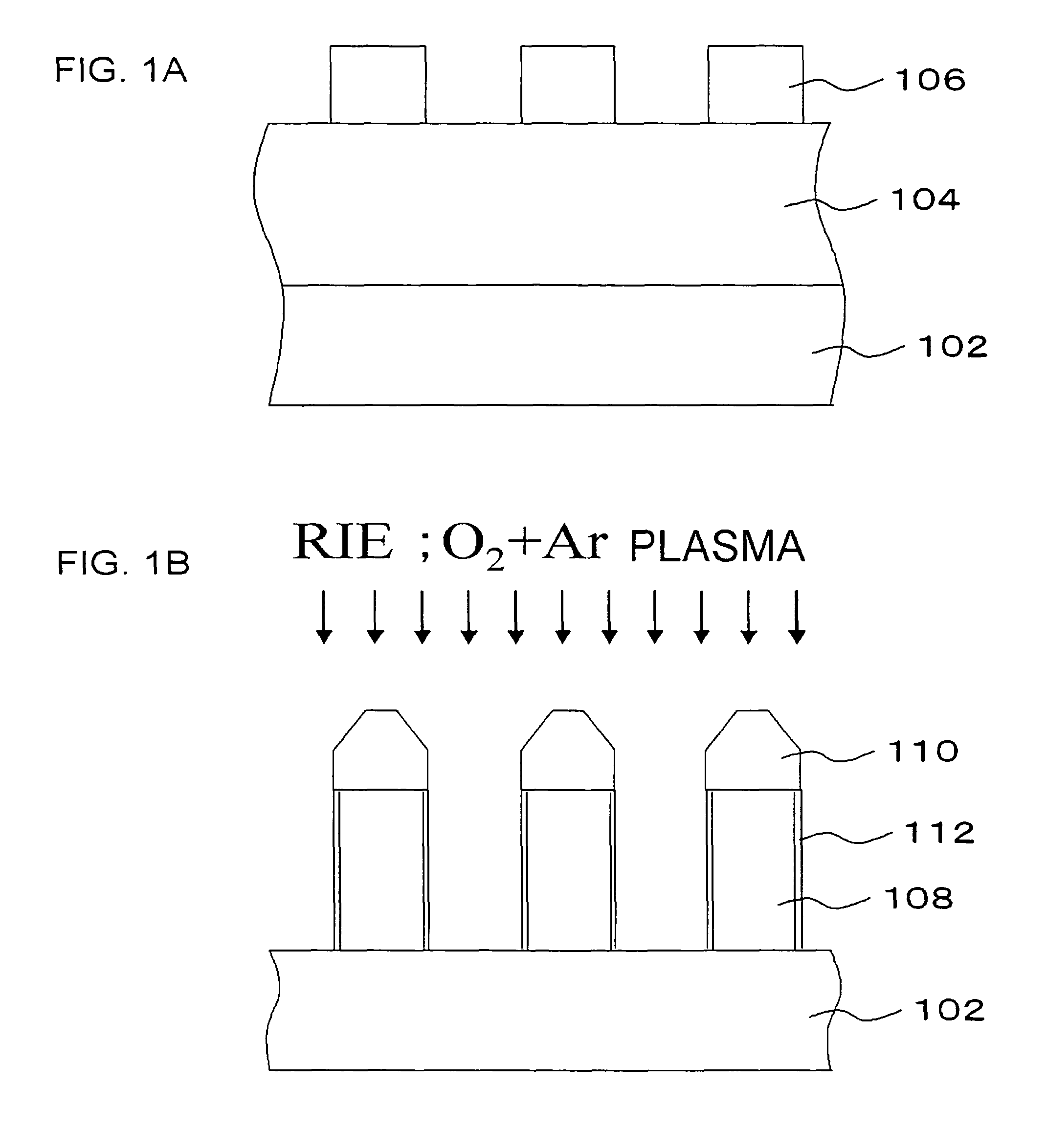
[0043]In the present embodiment, a case of employing a dual-layered resist will be described for an exemplary implementation. A process for patterning a multiple-layered resist film of the present embodiment includes the following operations:[0044](i) an operation for forming a lower layer resist film 104 on or over a semiconductor substrate;[0045](ii) an operation for forming a silicon-containing upper layer resist film on the lower layer resist film 104 (FIG. 1A);[0046](iii) an operation for patterning the silicon-containing upper layer resist film into a predetermined geometry (FIG. 1A); and[0047](iv) an operation for performing dry etching process for removing the lower layer resist film 104 through a mask of the patterned silicon-containing upper layer resist film 106 employing an etching gas containing oxygen (O2) gas and argon (Ar) gas at a pressure within a range of from 0.075 mTorr to 50 mTorr both inclusive (within a range of from about 0.01 Pa to about 6.7 Pa both inclusi...

second embodiment

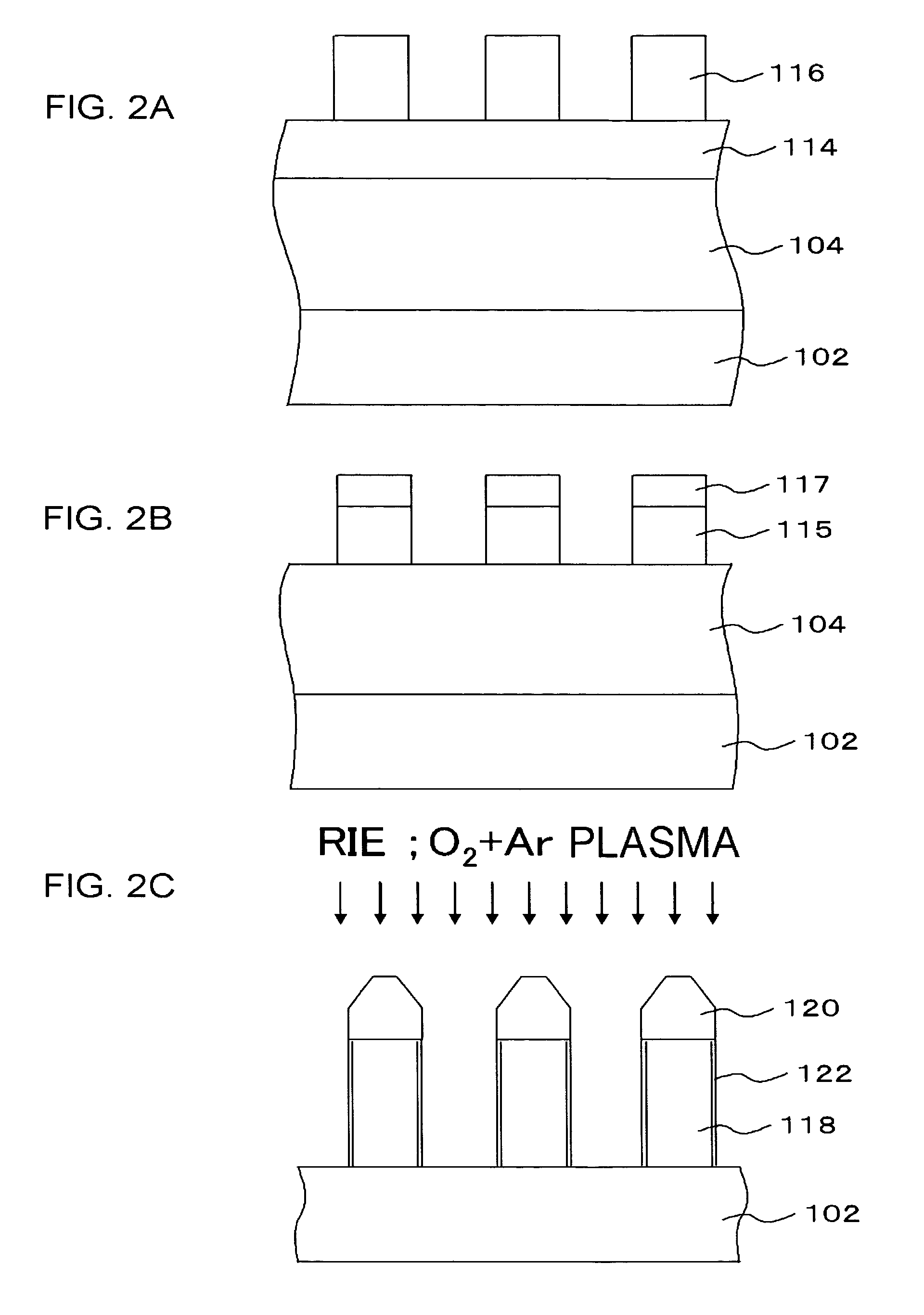
[0062]A process for patterning a multiple-layered resist film of the present embodiment includes the following operations:[0063](i) an operation for forming a lower layer resist film 104 on a semiconduct or substrate;[0064](ii) an operation for forming a silicon-containing upper layer resist film (multiple-layered film of silicon-containing intermediate layer and upper layer resist film) on the lower layer resist film 104 (FIG. 2A);[0065](iii) an operation for patterning the upper layer resist film into a predetermined geometry (FIG. 2A); and[0066](iv) an operation for performing dry etching process for removing the lower layer resist film 104 through a mask of the patterned silicon-containing upper layer resist film (multiple-layered film of silicon-containing intermediate layer 115 and upper layer resist film 117) employing an etching gas containing oxygen (O2) gas and argon (Ar) gas at a pressure within a range of from 0.075 mTorr to 50 mTorr both inclusive.

[0067]Following descri...

examples

Experiments 1 to 18

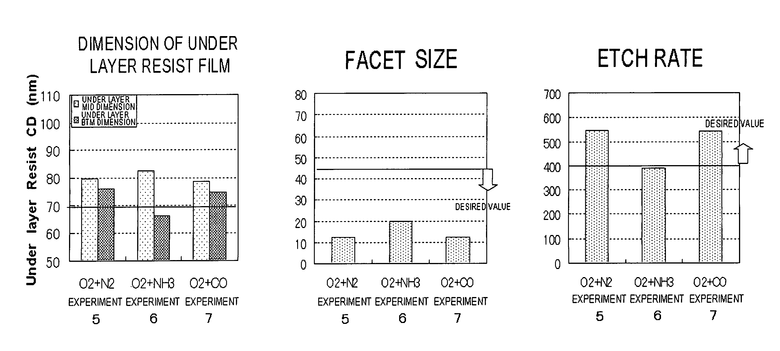
[0078]A multiple-layered resist film was etched by a same process as employed in first embodiment (FIGS. 1A and 1B). Here, structure of the multiple-layered resist film and the etch conditions were as follows:

[Multiple-layered Resist Film]

[0079]lower layer resist film: formed to a thickness of 300 nm (by employing a resist solution “B200” (commercially available from JSR Co., Ltd., Tokyo Japan));[0080]silicon-containing upper layer resist film: formed to a thickness of 90 nm (by employing a resist solution “JSF187” (commercially available from JSR Co., Ltd.));

[Exposure Condition for Upper Layer Resist Film][0081]F2 exposure (a pattern having line width of 70 nm / space of 70 nm is formed);

[Condition for Dry Etch for Lower Layer Resist Film][0082]etcher: dual-frequency RIE apparatus;[0083]etching gas: O2 gas, N2 gas, NH3 gas, CO gas, Ar gas (see FIG. 4);[0084]etching condition: pressure, flow rate of the etching gas and temperature of the semiconductor substrate are ...


PUM

PropertyMeasurementUnit
pressureaaaaaaaaaa
pressureaaaaaaaaaa
thicknessaaaaaaaaaa

Abstract

A method of patterning a multiple-layered resist film and a method of manufacturing a semiconductor device, which can provide an improved reliability of the semiconductor devices and a reduced operation time for an etch process, are provided. A method of patterning a multiple-layered resist film according to the present invention include: forming a lower layer resist film 104 on a semiconductor substrate; forming a silicon-containing upper layer resist film on the lower layer resist film 104; patterning the silicon-containing upper layer resist film into a predetermined geometry; and performing dry etching process for removing the lower layer resist film 104 through a mask of the patterned silicon-containing upper layer resist film 106 employing an etching gas containing oxygen (O2) gas and argon (Ar) gas at a pressure within a range of from 0.075 mTorr to 50 mTorr both inclusive.

Description

[0001]This application is based on Japanese patent application No. 2005-361,812, the content of which is incorporated hereinto by reference.BACKGROUND[0002]1. Technical Field[0003]The present invention relates to a method of patterning a multiple-layered resist film and a method of manufacturing a semiconductor device.[0004]2. Related Art[0005]In processes for manufacturing semiconductor devices, a material patterning is generally carried out by a lithography process to form patterned photoresist film and a successive dry etching process using the patterned photoresist film as a etching mask.[0006]As scaling down of semiconductor device proceeds, there needs to form device elements with a narrower pitch and a higher aspect ratio photoresist pattern, resulting in a reduced margin in lithgraphy process and a reduced mechanical stability of the patterned photoresist film against applied stress. One solution is to reduce the photoresist film thickness, but attended with insufficient etc...

Claims


Application Information

Patent Timeline
Patent Type & Authority Patents(United States)
IPC IPC(8): H01L21/84H01L21/00
CPCH01L21/31138H01L21/76802
Inventor SODA, EIICHI
Owner RENESAS ELECTRONICS CORP
Why Eureka
Try Eureka