Heterojunction photovoltaic cell

a photovoltaic cell and heterojunction technology, applied in the field of solar photovoltaic cells, can solve the problems of high manufacturing cost, complex fabrication process of dissimilar materials, poor mobility of such materials,

Inactive Publication Date: 2010-07-27
PALO ALTO RES CENT INC
View PDF9 Cites 18 Cited by
  • Summary
  • Abstract
  • Description
  • Claims
  • Application Information

AI Technical Summary

Problems solved by technology

The mobilities of such materials are often poor.
The fabrication process for junctions of dissimilar materials is usually complex, and the manufacturing cost is high.

Method used


Image

  • Heterojunction photovoltaic cell
  • Heterojunction photovoltaic cell
  • Heterojunction photovoltaic cell

Examples


Embodiment Construction

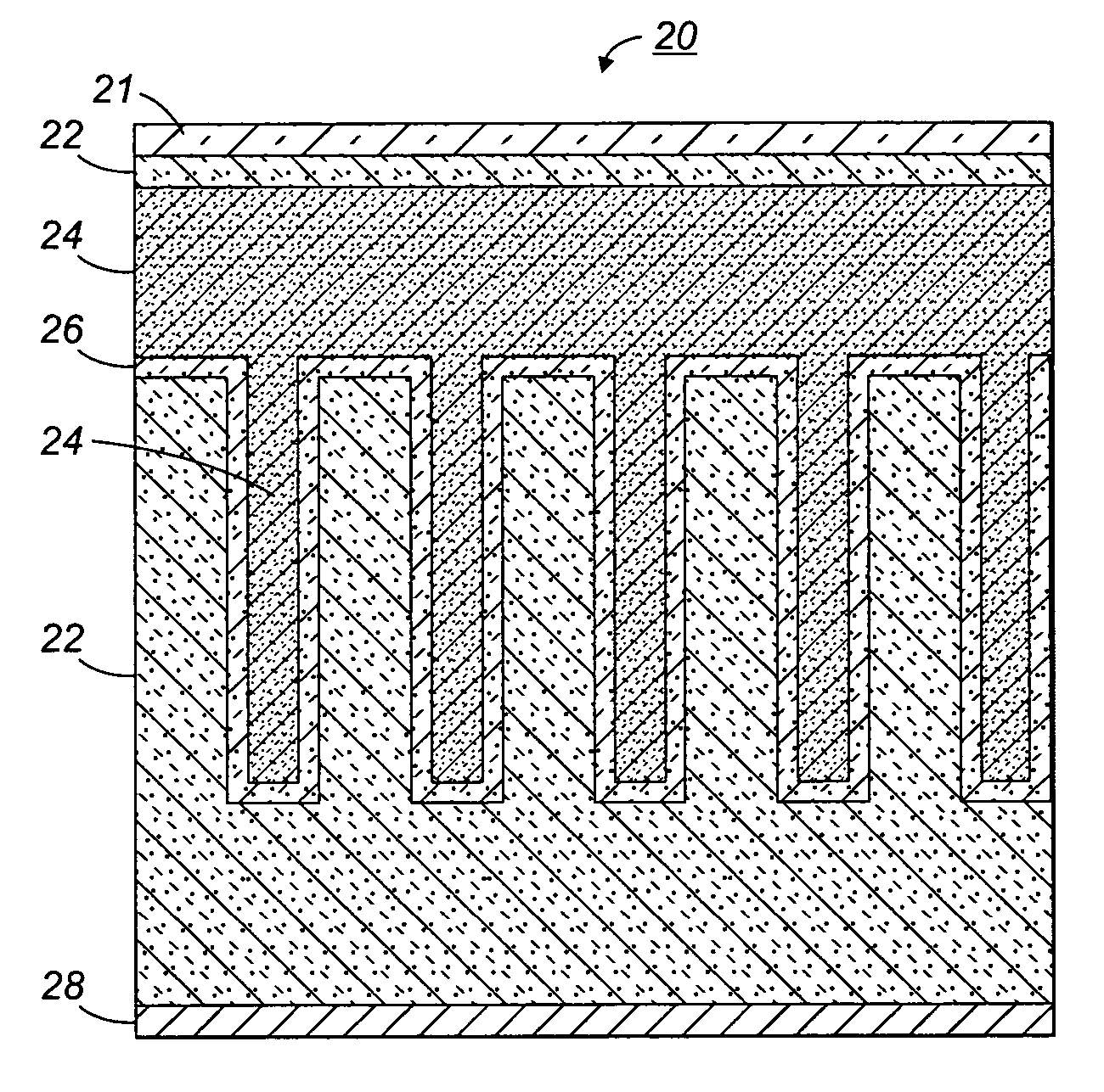
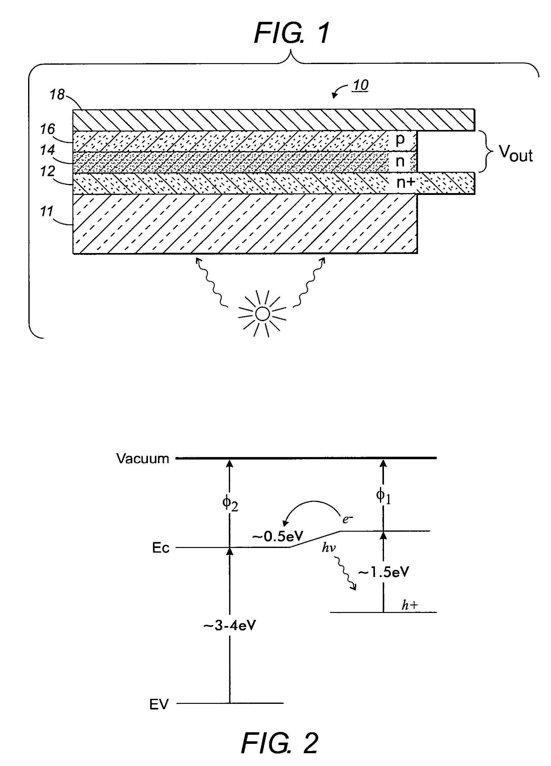
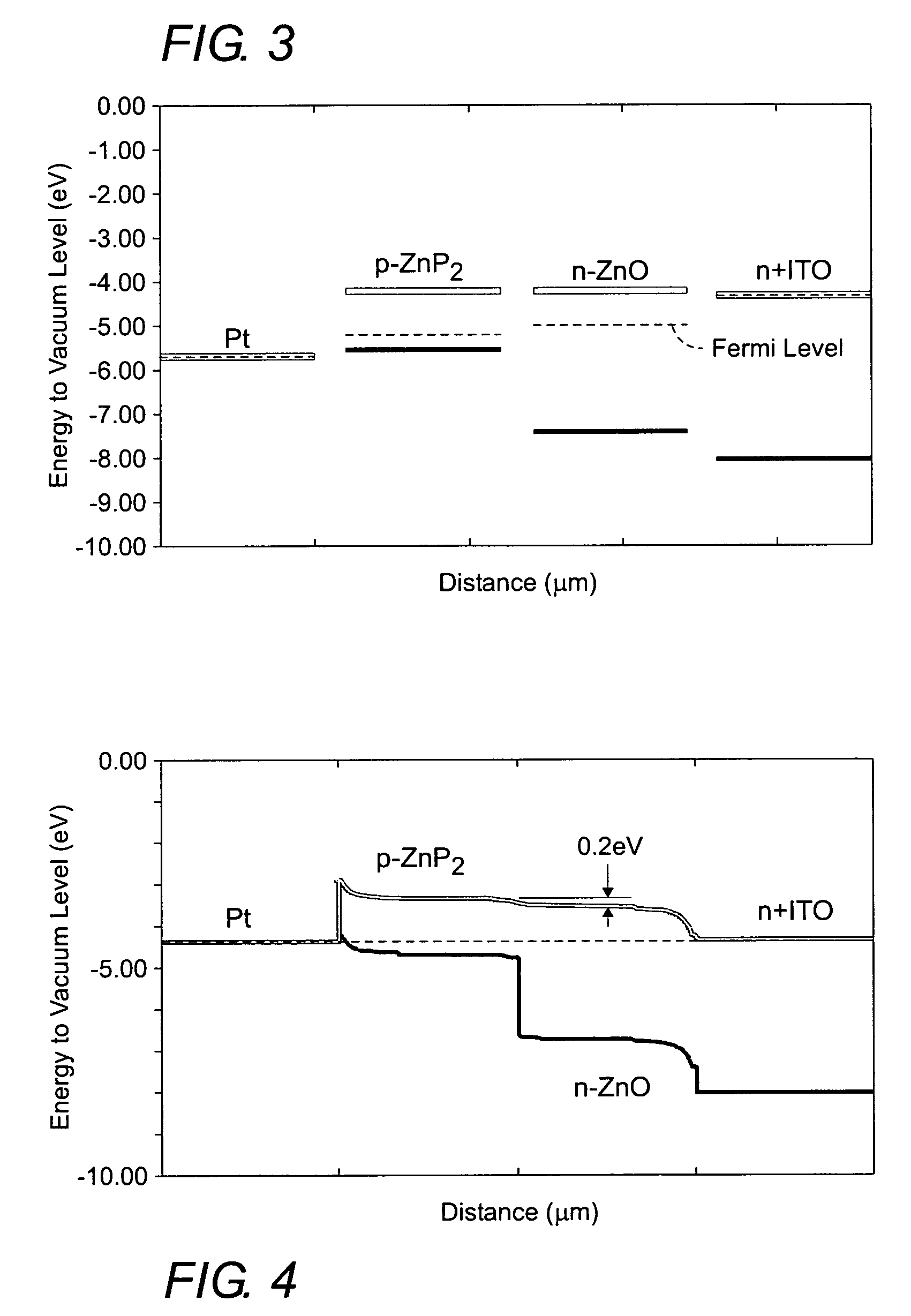
[0023]Referring now to FIG. 1, a photovoltaic cell 10 is illustrated. The photovoltaic cell 10 is a planar device and includes an electrically conductive support formed of an optically transparent substrate 11 and a transparent electrically conductive film 12.

[0024]The material used in the substrate 11 is not particularly limited and can be various kinds of transparent materials, and glass is preferably used.

[0025]The material used in the transparent electrically conductive film 12 is also not particularly limited, and it is preferred to use a transparent electrically conductive metallic oxide such as fluorinated tin oxide (SnO2:F), antimony-doped tin oxide (SnO2:Sb), indium tin oxide (ITO), aluminum-doped zinc oxide (AnO:Al) and gallium-doped zinc oxide (ZnO:Ga). The preferred materials for the transparent electroconductive film 12 are ITO or fluorinated tin oxide.

[0026]Examples of the method for forming the transparent electrically conductive film 12 on the substrate 11 include a ...


PUM


Abstract

In accordance with one aspect of the present disclosure, a solar photovoltaic device is disclosed. The semiconductor material of the solar photovoltaic device is a heterostructure of two different binary compounds of the same metal. One or both of the two different binary compounds of the same metal are doped so that they have a conduction band edge offset of greater than about 0.4 eV. The binary compound acting as the optical absorbing material of the solar photovoltaic device has a bandgap of about 1.0 eV to about 1.8 eV.

Description

BACKGROUND[0001]The present disclosure relates to semiconductor devices, and more particularly, to solar photovoltaic cells.[0002]A photovoltaic cell is a component in which light is converted directly into electrical energy.[0003]A heterojunction photovoltaic cell is one in which two dissimilar materials are used to generate band offsets in order to induce charge separation between generated electrons and holes.[0004]A heterojunction photovoltaic cell comprises at least one light-absorbing layer and a charge transport layer, as well as two electrodes. If the converted light is sunlight, the photovoltaic cell is a solar cell.[0005]For solar photovoltaic cells, one would ideally want to use low-cost, non-toxic and abundant source materials and process these materials at low temperature on inexpensive substrates. The mobilities of such materials are often poor. For example, thin film copper oxide (CuO) has a nearly ideal band gap (1.6 eV) for a solar photovoltaic device, but has a low...

Claims


Application Information

Patent Timeline
Patent Type & Authority Patents(United States)
IPC IPC(8): H01L31/00H01L25/00
CPCH01L31/03529H01L31/073H01L31/1828Y02E10/541Y02E10/543Y02P70/50
Inventor HANTSCHEL, THOMASLITTAU, KARL A.ELROD, SCOTT A.
Owner PALO ALTO RES CENT INC
Why Eureka
Try Eureka