On-chip spectroscopy

a total analysis and micro-chip technology, applied in the field of micro-total analysis systems, can solve the problems of loss of too much signal light to be able to practically detect the often weak optical response, and the connection to external or off-chip active optical elements, etc., to achieve the effect of reducing the height of the interconnection waveguide and being easy to integrate with the substra

Active Publication Date: 2010-07-27
SERSTECH
View PDF4 Cites 15 Cited by
  • Summary
  • Abstract
  • Description
  • Claims
  • Application Information

AI Technical Summary

Benefits of technology

[0011]The at least a part of the microfluidic channel, the slab waveguide and the grating may be one monolithic element and thus be fabricated using a simple manufacturing process, not requiring each part of the system to be manufactured in more or less separate process steps on the same substrate.
[0080]In a further aspect of the invention is provided a process for manufacturing the micro total analysis system by means of a moulding technique. In the process the main material is provided into a mould so that at least part of the microfluidic channel, the slab waveguide and the grating are formed in one piece. The moulding technique may be an injection moulding technique or an embossing moulding technique. The moulding may be a sequential moulding process. A sacrificial layer, or anti-sticktion layer may be provided to the mould so as to facilitate release of the moulded system.

Problems solved by technology

However, connection to external or off-chip active optical elements, such as light sources, detectors, spectroscopes, etc. is usually a demanding task, requiring precise alignment between the fluid handling chips and e.g. optical fibers connecting chip with the off-chip optical elements.
The lack of precise alignment may result in loss of too much signal light to be able to practically detect the often weak optical responses from the sample.

Method used


Image

  • On-chip spectroscopy
  • On-chip spectroscopy
  • On-chip spectroscopy

Examples


Embodiment Construction

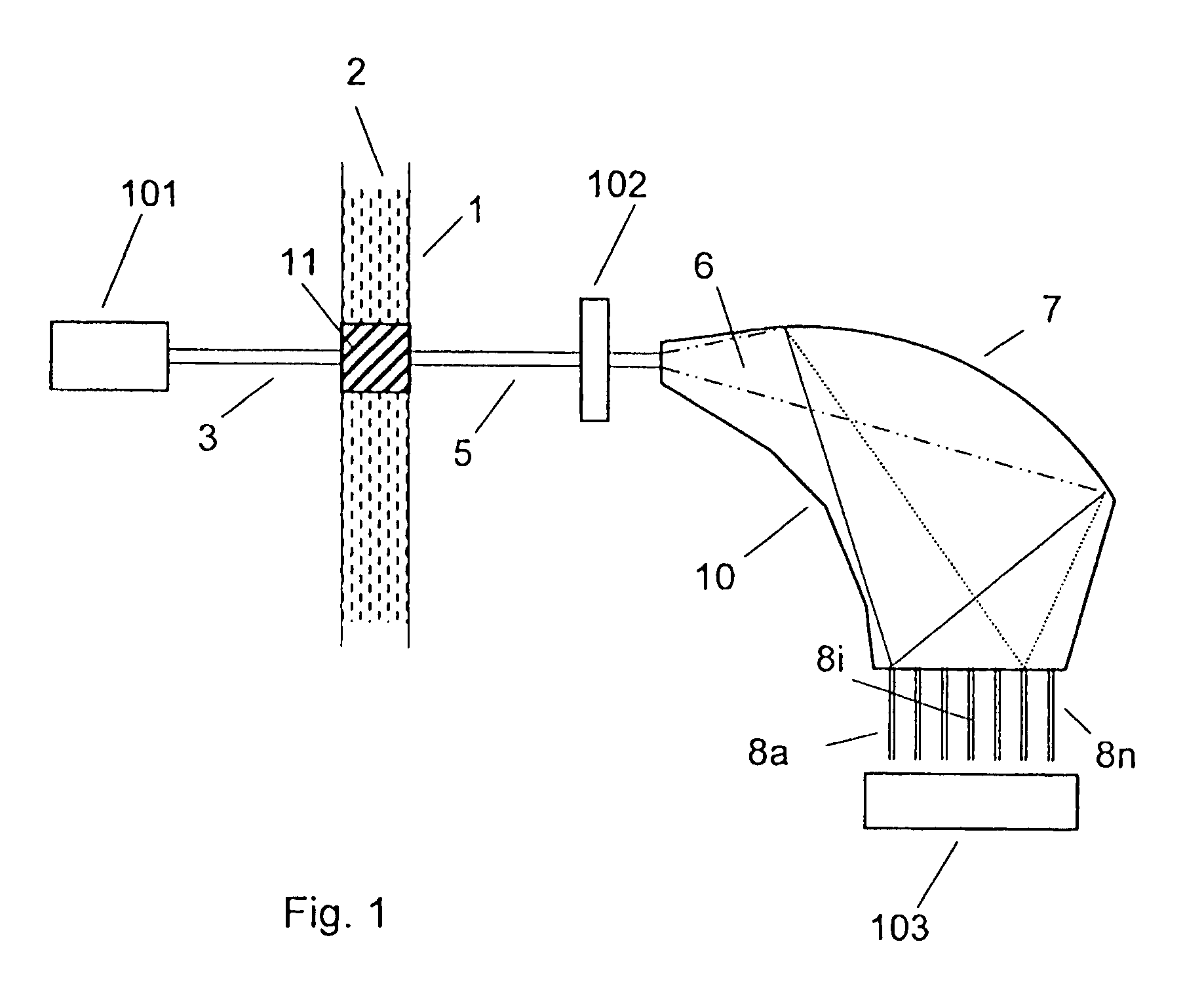
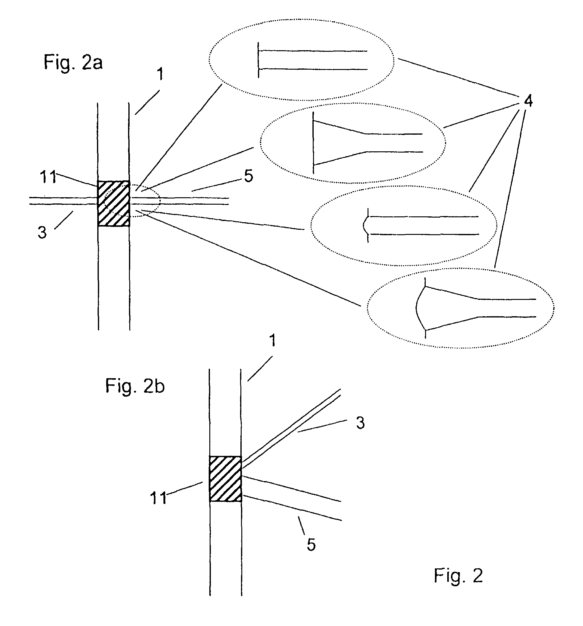
[0094]In FIG. 1, a micro total analysis system or at least a part of such a system is shown. The microfluidic channel 1 may comprise a fluid 2, being a gas or a liquid, to be analyzed.

[0095]The system in FIG. 1 is configured for absorption spectroscopy and a first optical waveguide 3 provides an incident electromagnetic wave to the fluid 2 in the analysation part 4, being substantially the exposed area of the channel. The incident electromagnetically wave is typically monochromatic light, such as a laser light. The electromagnetically wave may in a given embodiment be emitted from an external light source 101 or from a integrated light source 101. In a situation of fluorescence and Raman measurements may the electromagnetic wave also be launched through a transparent substrate or lid perpendicular to the channel 1. Typically, a part of the incident light will interact with the fluid and / or fluid components and be at least partly absorbed by the fluid or the fluid components. The res...


PUM

PropertyMeasurementUnit
angleaaaaaaaaaa
heightaaaaaaaaaa
heightaaaaaaaaaa

Abstract

The present invention relates to a micro total analysis system comprising a spectroscope and a method of manufacturing such a system comprising a spectroscope in a one step process. More over the invention relates to a method of analyzing a sample in the system. The micro total analysis system comprising a spectroscope provided on a substrate and for measuring electromagnetic radiation and at least one microfluidic channel. The spectroscope comprises: a slab waveguide for guiding electromagnetic waves towards a diffraction grating dispersing the electromagnetic waves into their component wavelengths, and output means for receiving the deflected electromagnetic waves. At least a part of the microfluidic channel, the slab waveguide and the grating comprises the same main material, such as a polymer material.

Description

FIELD OF INVENTION[0001]The present invention relates to a micro total analysis system comprising a spectroscope and a method of manufacturing such a system comprising a spectroscope in a one step process.BACKGROUND OF THE INVENTION[0002]Micro total analysis systems (μTAS) are becoming more widely used, and further still more features are built into such systems. The systems may be used for fast analysis of small volumes of fluids. The micro systems comprise microfluidic channels and reaction chambers and also functional elements such as mixers, pumps and separation may be integrated on the chip. The detection of properties of fluids or fluid components is dominated by optical methods, such as fluorescence detection or absorption spectroscopy.[0003]Typically, the optical systems are provided at a separate device or only partly integrated with the fluid handling system. There has been a strong effort to integrate parts of the optical system, such as waveguides with the fluid handling...

Claims


Application Information

Patent Timeline
Patent Type & Authority Patents(United States)
IPC IPC(8): G01J3/18G01N21/65G01J3/44B01L3/00G01J3/28G01N21/01
CPCG01J3/18G01J3/28G01J3/44G01N21/05G01N21/645G01N21/658G01J3/0256G01N2021/0346
Inventor HUBNER, JORGJORGENSEN, ANDERS MICHAELANHOJ, THOMAS AAROEZAUNER, DAN ANKER
Owner SERSTECH
Why Eureka
Try Eureka