Flash memory system and programming method performed therein

a memory system and programming method technology, applied in the field of memory devices and programming methods performed therein, can solve the problems of cluster gap generation, limited bandwidth, and limit as to how much data recording speed can be improved, and achieve the effect of increasing the overall bandwidth and data recording speed without increasing the size of data

Inactive Publication Date: 2010-07-27
SAMSUNG ELECTRONICS CO LTD
View PDF8 Cites 55 Cited by
  • Summary
  • Abstract
  • Description
  • Claims
  • Application Information

AI Technical Summary

Benefits of technology

[0013]The present invention provides a flash memory system capable of increasing the overall bandwidth and data recording speed without increasing the size of data to be transmitted by a host, and a programming method performed in the flash memory system.

Problems solved by technology

However, in the related art, even when an interleaving process is applied between chips included in the same channel or when the number of the channel is increased, there is a limit as to how much the data recording speed can be improved.
When data is recorded to a plurality of memory cell arrays or flash memory chips included in a single channel according to an interleaving process, a bandwidth is limited due to the recording time tWC of the flash memory chip itself.
Also, a cluster gap may be generated due to the increase in size of the unit of a physical data access rate.

Method used


Image

  • Flash memory system and programming method performed therein
  • Flash memory system and programming method performed therein
  • Flash memory system and programming method performed therein

Examples


Embodiment Construction

[0028]The present invention will now be described more fully with reference to the accompanying drawings, in which exemplary embodiments of the invention are shown.

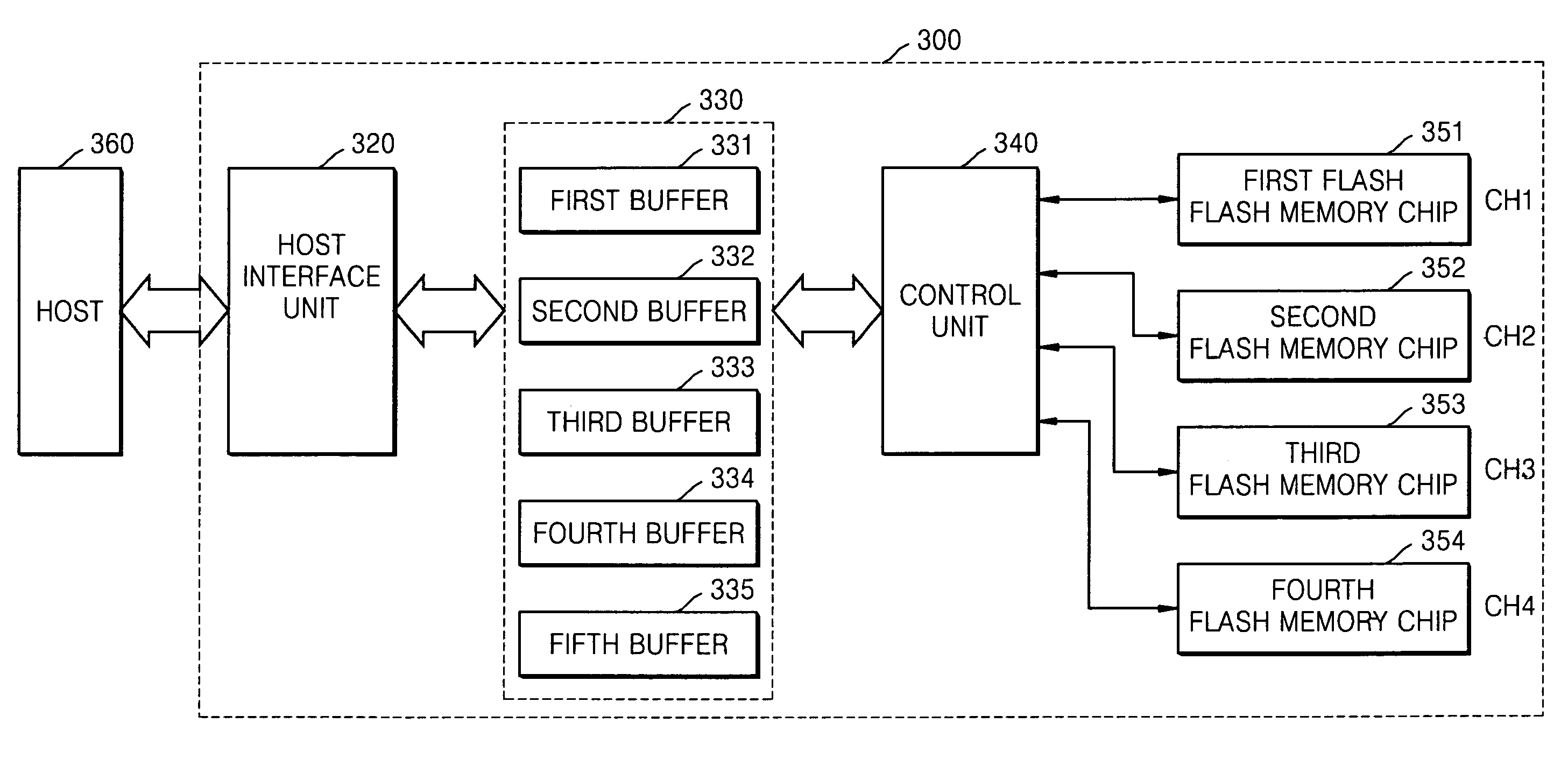
[0029]FIG. 3 is a block diagram of a flash memory system 300 according to an exemplary embodiment of the present invention. Referring to FIG. 3, the flash memory system 300 includes a host interface unit 320, a buffer unit 330 including a plurality of buffers 331 through 335, a control unit 340, and a plurality of flash memory chips 351, 352, 353, and 354. The flash memory chips 351, 352, 353, and 354 form channel units CH1, CH2, CH3, and CH4, respectively. However, the present invention is not limited to this configuration. That is, each of the channel units CH1, CH2, CH3, and CH4 may further include at least one flash memory chip.

[0030]The host interface unit 320 sequentially transmits page data received from the host 360 to the buffers 331 through 335, according to the sequence in which the page data is transmitted by ...


PUM


Abstract

Provided are a flash memory system and a programming method performed in the flash memory system. The flash memory system includes a buffer unit including a plurality of buffers, and temporarily storing data transmitted by a host; a plurality of channel units each including at least one flash memory chip that includes a plurality of memory cell arrays; and a control unit which controls the data stored in the buffer unit to be sequentially transmitted to the channel units and the transmitted data to be recorded to the memory cell arrays of the flash memory chips in the channel units.

Description

CROSS-REFERENCE TO RELATED PATENT APPLICATION[0001]This application claims priority from Korean Patent Application No. 10-2006-0079947, filed on Aug. 23, 2006, in the Korean Intellectual Property Office, the disclosure of which is incorporated herein in its entirety by reference.BACKGROUND OF THE INVENTION[0002]1. Field of the Invention[0003]Systems and methods consistent with the present invention relate to a memory device and a programming method performed therein, and more particularly, to a flash memory system capable of increasing the overall bandwidth and data recording speed by achieving simultaneous performance of sequential transmission of data to each channel unit and storage of data transmitted from a host by using a plurality of buffers, and a programming method performed in the flash memory system.[0004]2. Description of the Related Art[0005]Flash memories, which are non-volatile memories capable of electrically deleting or re-recording data, are classified into a NOR t...

Claims


Application Information

Patent Timeline
Patent Type & Authority Patents(United States)
IPC IPC(8): G06F12/00
CPCG11C16/10G06F9/06G06F12/00
Inventor KANG, SHIN-WOOKLEE, DONG-WOO
Owner SAMSUNG ELECTRONICS CO LTD
Why Eureka
Try Eureka