Image sensor and method for manufacturing the same

a technology of image sensor and manufacturing method, which is applied in the field of image sensor, can solve the problems of degrading the sensitivity of an image sensor and the photodiode not absorbing all of the light, and achieve the effects of improving the sensitivity of the image sensor, minimizing light reflection, and maximizing light absorption

Inactive Publication Date: 2010-08-03
DONGBU ELECTRONICS CO LTD
View PDF7 Cites 2 Cited by
  • Summary
  • Abstract
  • Description
  • Claims
  • Application Information

AI Technical Summary

Benefits of technology

[0020]The present invention has been made to solve the above problem(s), and therefore, it is an object of the present invention to provide an image sensor and a method for manufacturing the same, capable of improving the sensitivity of the image sensor by irregularly forming the surface of a photodiode so as to induce diffused reflection and enhance light absorption.
[0023]The sensitivity improvement of an image sensor is the most important target to be achieved. In order to improve the sensitivity of the image sensor, although the thickness of an insulating layer and a micro-lens are important variables, a light absorption coefficient of the photodiode for detecting light should also be considered. In this case, the light absorption coefficient relates to the amount of absorbed light in the incident light. As a result, the reflection of light is minimized, and the absorption of light is maximized, so that the sensitivity of the image sensor can be improved even when the thicknesses of the insulating layer and the micro-lens are the same. Thus, the photodiodes generally have a surface roughness sufficient to increase a light absorption coefficient of the photodiodes relative to otherwise identical photodiodes having an unroughened surface.
[0024]To this end, according to the present invention, a sputter etching process is performed with respect to the surface of the photodiodes so as to obtain a rough surface thereon, thereby improving the light absorption coefficient of the photodiodes. Accordingly, a surface area capable of absorbing light is increased, and reflected light may be absorbed after its reflection, thereby improving the sensitivity of the photodiode as compared with that of a conventional photodiode having a relatively planar surface.
[0025]Therefore, the light absorption coefficient of the photodiode is enhanced, so the quality of an image sensor product can be improved.

Problems solved by technology

However, the conventional photodiode does not absorb all of the light, but reflects some of the light.
The reflected light may degrade the sensitivity of an image sensor.

Method used


Image

  • Image sensor and method for manufacturing the same
  • Image sensor and method for manufacturing the same
  • Image sensor and method for manufacturing the same

Examples


Embodiment Construction

[0032]Hereinafter, an image sensor and a method for manufacturing the image sensor according to the present invention will be described with reference to accompanying drawings.

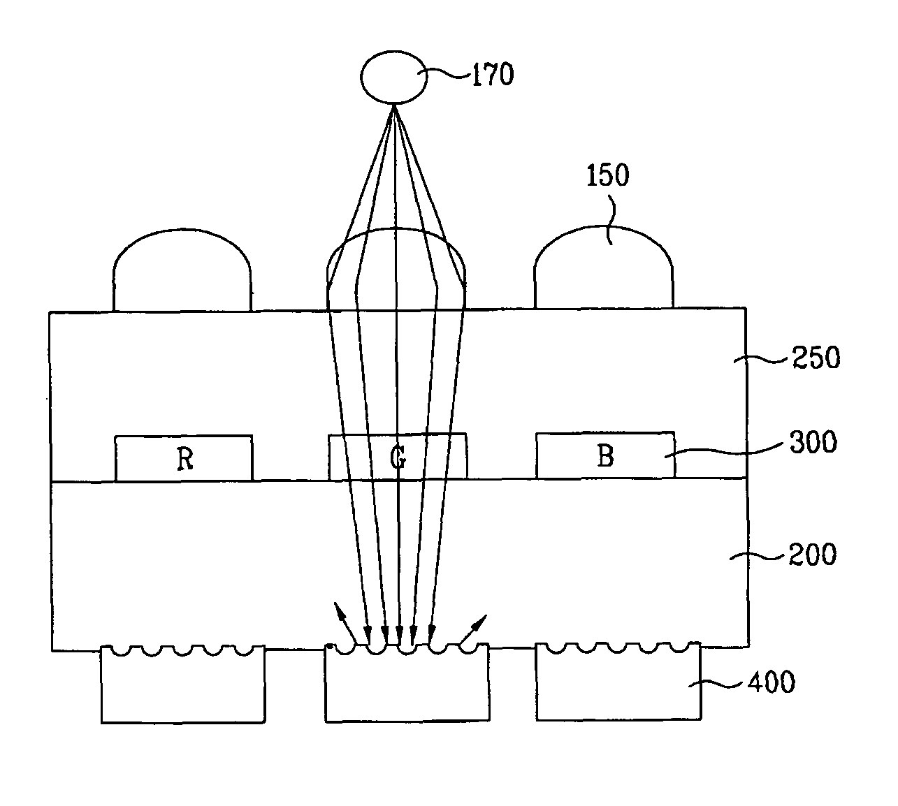
[0033]FIG. 4 is a view showing an image sensor according to the present invention. FIG. 5 is a view showing the path of light in a photodiode according to the present invention. FIGS. 6A to 6C are sectional views showing a method for forming an image sensor according to the present invention.

[0034]As shown in FIG. 4, an image sensor according to the present invention includes a plurality of photodiodes 400, and each of the photodiodes 400 has a rough surface. In order to make the surface of the photodiode rough, a sputter etching process may be performed.

[0035]A dielectric layer 200 (e.g., an inter-layer dielectric) is formed on a semiconductor substrate 100 including the photodiodes 400, and a color filter layer 300 is formed on the dielectric layer 200 such that the color filter layer 300 corresponds to the ...


PUM


Abstract

Disclosed are an image sensor and a method for manufacturing the same, capable of increasing a light absorbing coefficient by forming a rough surface on a photodiode. The image sensor includes a semiconductor substrate with a plurality of photodiodes thereon having rough upper surfaces, a dielectric layer on the semiconductor substrate, a color filter layer on the dielectric layer, a planarization layer on an entire surface of the semiconductor substrate including the color filter layer, and a plurality of micro-lenses formed on the planarization layer to correspond to the color filter layer.

Description

BACKGROUND OF THE INVENTION[0001]1. Field of the Invention[0002]The present invention relates to an image sensor. More particularly, the present invention relates to an image sensor and a method for manufacturing the same, capable of improving the sensitivity of a photodiode by making a rough surface on the photodiode such that the light absorption coefficient of the photodiode can be enhanced and light reflected from the photodiode can be prevented from being discharged through an upper layer.[0003]2. Description of the Related Art[0004]In general, image sensors are semiconductor devices for converting optical images into electric signals, and are generally classified into a charge coupled device (CCD) image sensor and a complementary metal oxide semiconductor (CMOS) image sensor.[0005]The CMOS image sensor includes aphotodiode for detecting irradiated light and a logic circuit for converting detected light into electric signals which can be processed (e.g., as data). As the quanti...

Claims


Application Information

Patent Timeline
Patent Type & Authority Patents(United States)
IPC IPC(8): H01L21/00
CPCH01L27/1462H01L27/14625H01L27/14685H01L27/146
Inventor KIM, SANG CHULHAN, JAE WON
Owner DONGBU ELECTRONICS CO LTD
Why Eureka
Try Eureka