Semiconductor memory device including a contact with different upper and bottom surface diameters and manufacturing method thereof

a memory device and semiconductor technology, applied in the direction of transistors, solid-state devices, capacitors, etc., can solve the problems of reducing the resistance value of the capacitive value, reducing the area on the semiconductor substrate which can be allocated to the storage capacitor, and conventionally difficult to prevent so as to reduce the resistance value of the capacitor contact, the effect of preventing the occurrence of shorting defects

Inactive Publication Date: 2010-08-10
LONGITUDE SEMICON S A R L
View PDF7 Cites 1 Cited by
  • Summary
  • Abstract
  • Description
  • Claims
  • Application Information

AI Technical Summary

Benefits of technology

[0010]It is therefore an object of the present invention to provide a semiconductor memory device can prevent occurrence of shorting defects while decreasing a resistance value of a capacitor contact, and a manufacturing method thereof.
[0013]According to the present invention, pillars exist between the cell contacts and the capacitor contacts, and therefore, depths of the capacitor contacts can be made correspondingly shorter. Thereby, the bottom diameters of the capacitor contacts can be enlarged as compared to those in the conventional case, and the capacitor contacts can be formed precisely. Accordingly, it becomes possible to prevent occurrence of shorting defects while decreasing the resistance value of the capacitor contact.

Problems solved by technology

However, when the memory cell of the DRAM is miniaturized, an area on a semiconductor substrate which can be allocated to the storage capacitor becomes small.
Accordingly, it is conventionally difficult to prevent occurrence of shorting defects while decreasing the resistance value of the capacitive value.

Method used


Image

  • Semiconductor memory device including a contact with different upper and bottom surface diameters and manufacturing method thereof
  • Semiconductor memory device including a contact with different upper and bottom surface diameters and manufacturing method thereof
  • Semiconductor memory device including a contact with different upper and bottom surface diameters and manufacturing method thereof

Examples


Embodiment Construction

[0029]Preferred embodiments of the present invention will now be explained in detail with reference to the drawings.

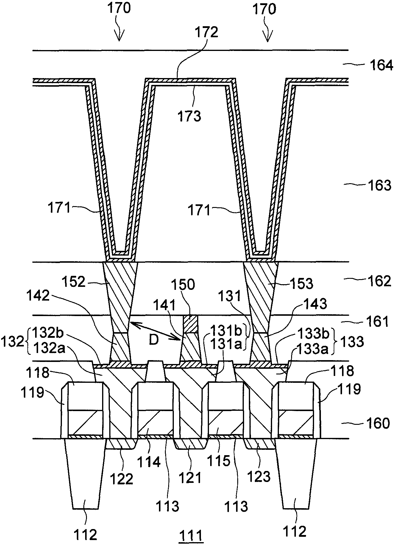
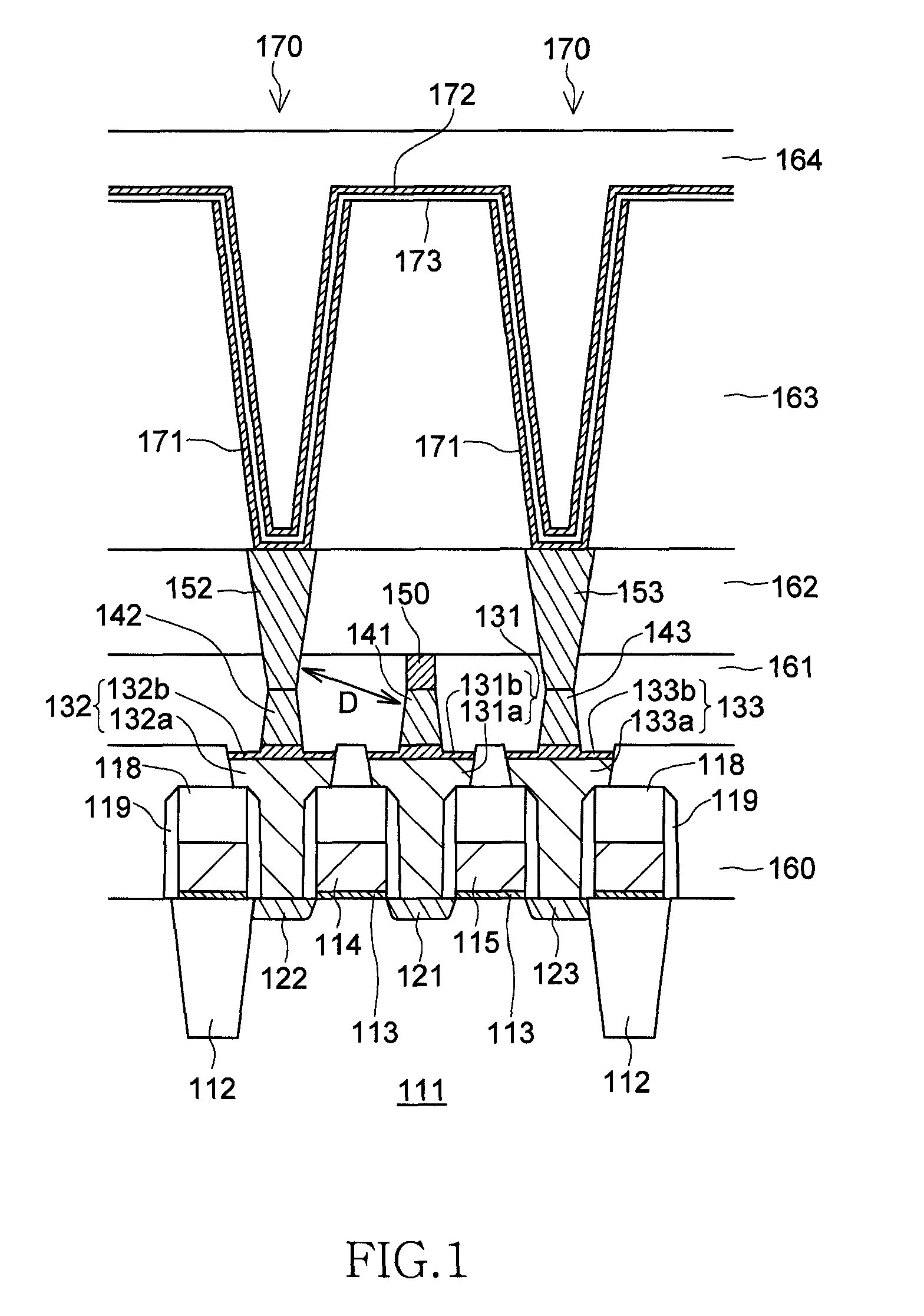
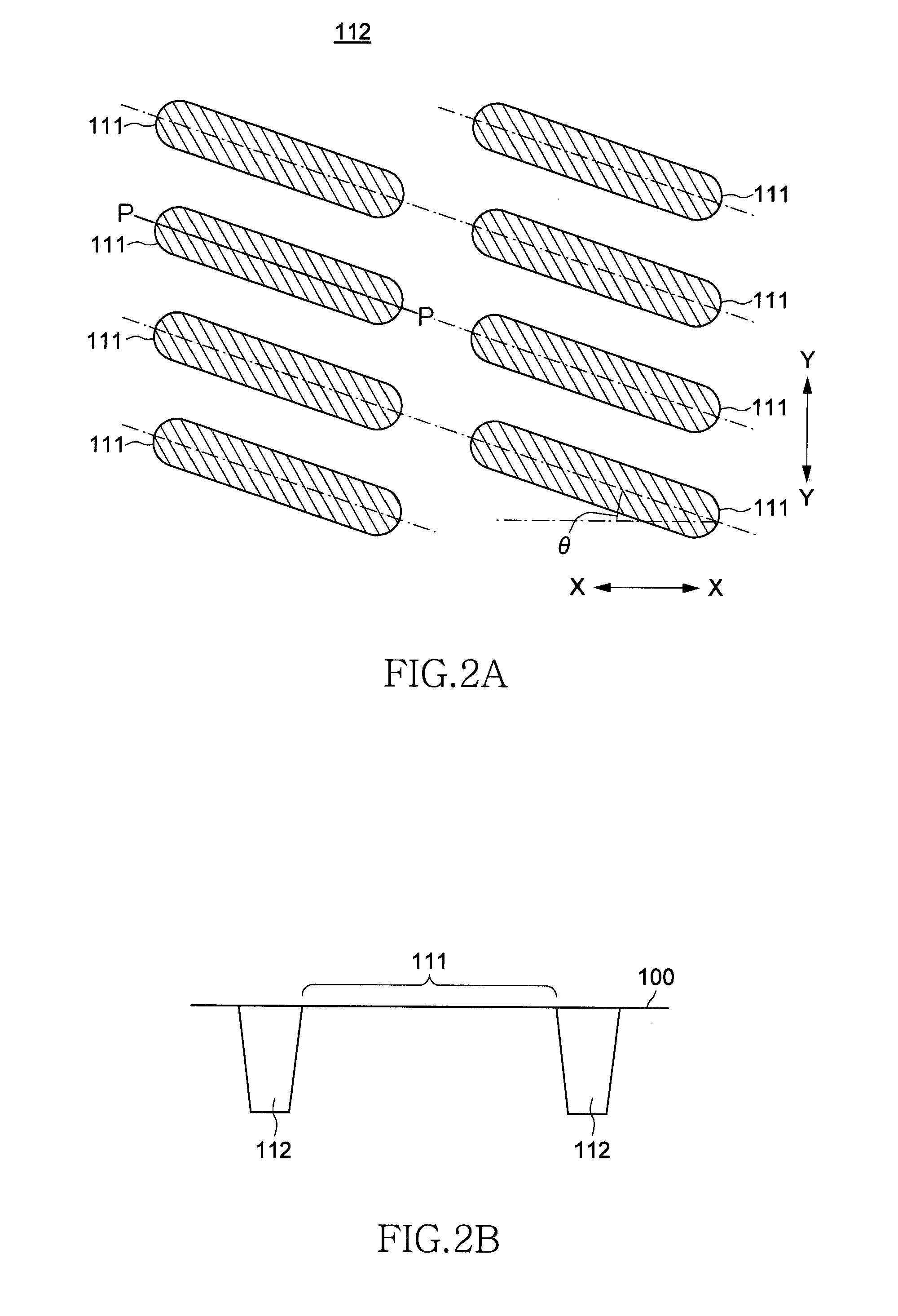
[0030]FIG. 1 is a schematic cross-sectional view showing a structure of a semiconductor memory device according to a preferred embodiment of the present invention. The semiconductor memory device according to the embodiment is a DRAM. One active region 111 divided by element isolation regions 112 is formed with two memory cells.

[0031]As shown in FIG. 1, one active region 111 divided by the element isolation regions 112 is formed with three diffusion regions 121 to 123. Above the diffusion regions 121 and 122 are adjacent to each other. A gate electrode 114 is formed via a gate insulating film 113 on the active region 111, whereby one cell transistor is configured. Accordingly, upon activation of the gate electrode 114, the diffusion regions 121 and 122 adjacent to each other are electrically connected.

[0032]Similarly, above the diffusion regions 121 and 123 are adjacen...


PUM


Abstract

A semiconductor memory device includes diffusion regions formed in an active region; cell contacts connected to the diffusion regions, respectively; pillars connected to the cell contacts, respectively; a bit line connected to the pillar; capacitor contacts connected to the pillars, respectively; and storage capacitors connected to the capacitor contacts, respectively. Accordingly, the pillars exist between the cell contacts and the capacitor contacts, and thus, depths of the capacitor contacts are made correspondingly shorter. Therefore, it becomes possible to prevent occurrence of shorting defects while decreasing resistance values of the capacitor contacts.

Description

TECHNICAL FIELD[0001]The present invention relates to a semiconductor memory device and a manufacturing method thereof, and, more particularly relates to a memory cell of a DRAM (Dynamic Random Access Memory) and a manufacturing method thereof.BACKGROUND OF THE INVENTION[0002]In the DRAM, which is one of semiconductor memory devices, a memory cell is configured by one cell transistor and one storage capacitor, and thus, a higher storage capacity can be obtained as compared to other semiconductor memory devices. However, when the memory cell of the DRAM is miniaturized, an area on a semiconductor substrate which can be allocated to the storage capacitor becomes small. Thus, to secure a sufficient capacity value, it is required that the storage capacitor have a three-dimensional structure. As a storage capacitor having a three-dimensional structure, a stacked capacitor is well known (see Japanese Patent Applications Laid-open Nos. 2006-120832, 2000-77620, and 2003-264196).[0003]FIG. 1...

Claims


Application Information

Patent Timeline
Patent Type & Authority Patents(United States)
IPC IPC(8): H01L21/8242
CPCH01L21/31116H01L21/31138H01L21/32136H01L21/32139H01L21/76849H01L21/76895H01L27/10855H01L28/91H01L21/76885Y10S257/906Y10S257/908H10B12/0335
Inventor OHUCHI, MASAHIKO
Owner LONGITUDE SEMICON S A R L
Why Eureka
Try Eureka