Monolithic semiconductor microwave switch array

a semiconductor and microwave switch technology, applied in the field of semiconductor switches, can solve the problems of degrading the performance of the switch and slot line, and affecting the operation of the array as a whole, so as to achieve the effect of reducing or eliminating the effect of potential

Active Publication Date: 2010-08-17
SIERRA NEVADA CORP
View PDF5 Cites 5 Cited by
  • Summary
  • Abstract
  • Description
  • Claims
  • Application Information

AI Technical Summary

Benefits of technology

[0013]As will be better appreciated from the detailed description below, an array of semiconductor microwave switches constructed in accordance with this disclosure minimizes, or at least substantially reduces, the deleterious effects of plasma diffusion, as described above.

Problems solved by technology

One disadvantage of the prior art semiconductor switch array 10, as described above, is that the plasma created by the application of the potential across the electrodes of each PIN junction switch is not effectively confined to the area in the vicinity of that switch.
Thus, in the switch array 10, the plasma created by each PIN junction switch tends to diffuse across the surface of the substrate 12, so that it may “contaminate” other switches and slotlines in the array thereby degrading the performance of those switches and slotlines, and compromising the functioning of the array as a whole.
Moreover, within each switch, the plasma tends to diffuse along the length of the slotline, away from the electrodes, thereby degrading the performance of the slotline controlled by that switch.

Method used


Image

  • Monolithic semiconductor microwave switch array
  • Monolithic semiconductor microwave switch array
  • Monolithic semiconductor microwave switch array

Examples


Embodiment Construction

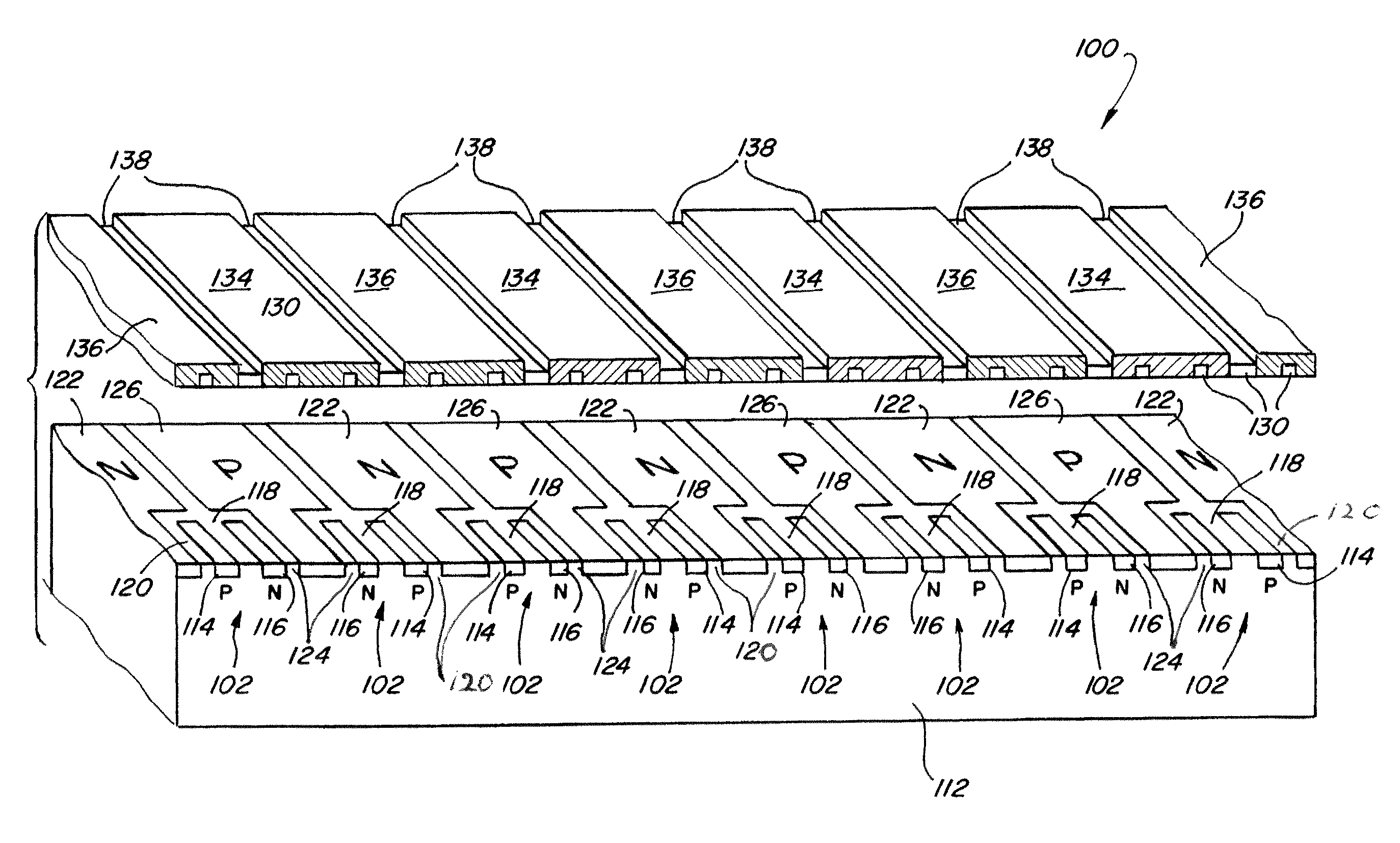
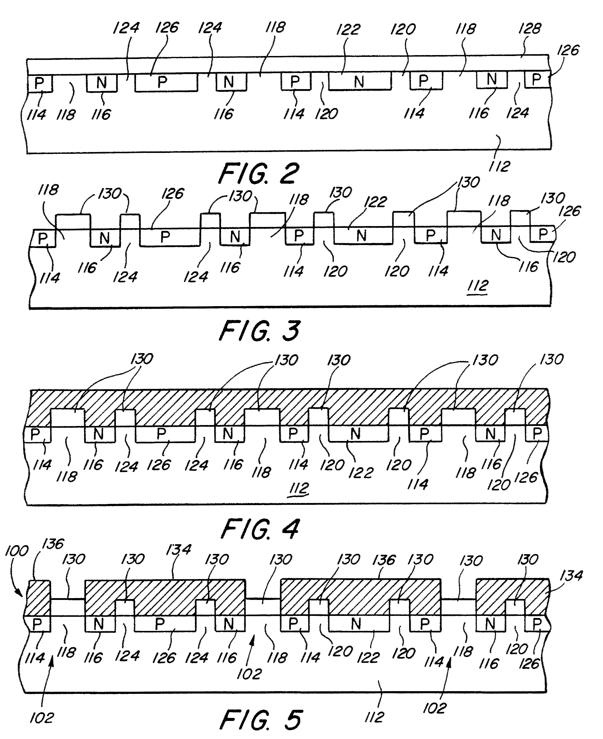
[0019]FIGS. 5, 6, and 7 show a monolithic array 100 of semiconductor microwave switches 102, in accordance with the present disclosure, while FIGS. 2, 3, and 4 show several steps in the fabrication of the array 100. The array 100 of the switches 102 is formed on a wafer or substrate 112 of undoped semiconductor material, such as Si, Ge, or GaAs. Each of the switches 102 is a PIN junction switch, comprising a first PIN junction provided by a first P-doped region that serves as a primary P-type electrode 114 and a first N-doped region that serves as a primary N-type electrode 116, the primary electrodes 114, 116 being separated by an insulative region 118 of undoped substrate material. A second PIN junction is provided by forming a second N-doped region separated from the primary P-type electrode 114 by a first isolation gap 120, the second N-doped region serving as a secondary N-type electrode 122. A third PIN junction is provided by forming a second P-doped region separated from the...


PUM


Abstract

A microwave switch array includes a plurality of microwave slotlines, each of which is controlled by a semiconductor switch including a first PIN junction formed by a primary P-type electrode and a primary N-type electrode separated by the slotline. The switches inject a plasma into the slotline in response to a potential applied across the first PIN junction. Each of the switches includes a second PIN junction between the primary P-type electrode and a secondary N-type electrode, and a third PIN junction between the primary N-type electrode and a secondary P-type electrode. Metal contacts connect the primary P-type electrode and the secondary N-type electrode across second PIN junction, and the primary N-type electrode and the secondary P-type electrode across the third PIN junction. The secondary electrodes extract plasma that diffuses away from the first PIN junction, thereby minimizing the performance degrading effects of plasma diffusion.

Description

CROSS-REFERENCE TO RELATED APPLICATION[0001]Not ApplicableFEDERALLY SPONSORED RESEARCH OR DEVELOPMENT[0002]Not ApplicableBACKGROUND[0003]The present disclosure relates to semiconductor switches for switching, controlling and / or directing electromagnetic radiation, particularly microwave radiation in the portion of the spectrum known as “millimeter waves.” Such millimeter wave radiation typically is employed in many radar applications, particularly collision avoidance radar used in various types of vehicles and craft.[0004]Semiconductor microwave switches are known in the art, and have been employed in such applications as steerable or directional antennas, especially dielectric waveguide antennas used to send and receive steerable millimeter wave beams in various types of radar devices, such as collision avoidance radars. In such antennas, semiconductor switches may be employed to provide an antenna element with an evanescent coupling edge having a selectively variable coupling geom...

Claims


Application Information

Patent Timeline
Patent Type & Authority Patents(United States)
IPC IPC(8): H01L21/329
CPCH01L27/0814H01L29/868H01P1/15H01L29/20
Inventor MANASSON, VLADIMIRLITVINOV, VLADIMIR I.SADOVNIK, LEVAVAKIAN, ARAMAIS
Owner SIERRA NEVADA CORP
Why Eureka
Try Eureka