Method and system for controllable deposition of nanoparticles on a substrate

a nanoparticle and substrate technology, applied in the field of microelectronic device manufacturing, can solve the problems of limiting the application of metal-semiconductor devices, damaging the metal-coated polymer stamp,

Inactive Publication Date: 2010-08-24
MARYLAND UNIV OF
View PDF1 Cites 1 Cited by
  • Summary
  • Abstract
  • Description
  • Claims
  • Application Information

AI Technical Summary

Benefits of technology

[0011]It is an object of the present invention to provide a method and system for controlling the deposition of nanoparticles on a substrate, in which a stable deposition pattern can be formed on a substrate which possesses thermal as well as chemical stability and can be fabricated with traditional microelectronic manufacturing methods.
[0012]It is a further object of the present invention to provide a technique for precisely directing the motion and controllable deposition of charged metal nanoparticles from the gas phase onto substrates by using the electrostatic force generated by reverse biased p-n junction patterned on the substrate.

Problems solved by technology

However, the gas-phase patterning of nanoparticles on a charge-patterned substrate has many technical shortcomings, including: (i) failure to attain stable patterns causing the change of the deposition pattern during the particle deposition process, (ii) high possibility for damaging the metal-coated polymer stamp during the charging process, as well as (iii) the necessity of using an insulated surface on the substrate which limits its applications especially for metal-semiconductor devices.

Method used


Image

  • Method and system for controllable deposition of nanoparticles on a substrate
  • Method and system for controllable deposition of nanoparticles on a substrate
  • Method and system for controllable deposition of nanoparticles on a substrate

Examples


Embodiment Construction

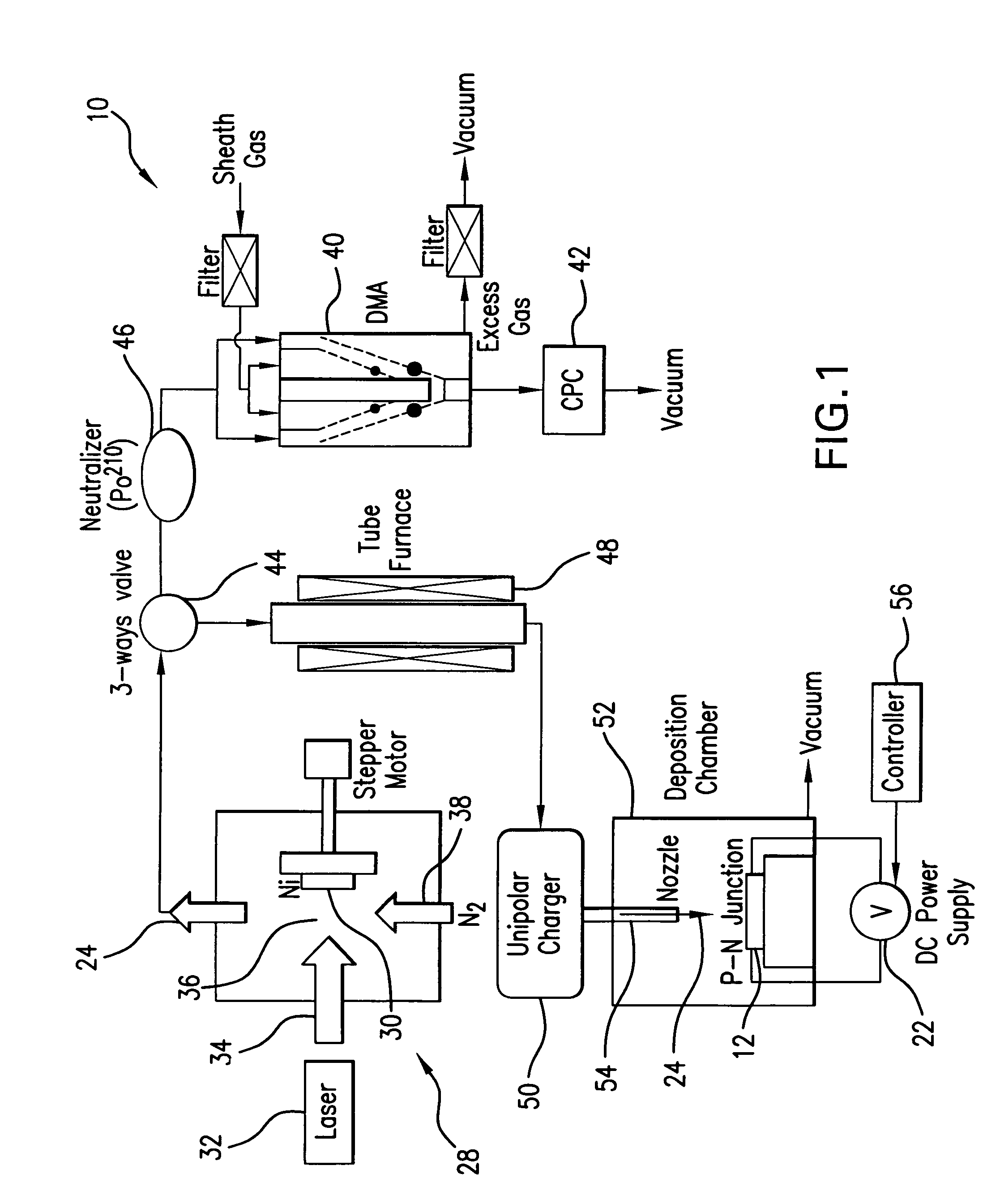
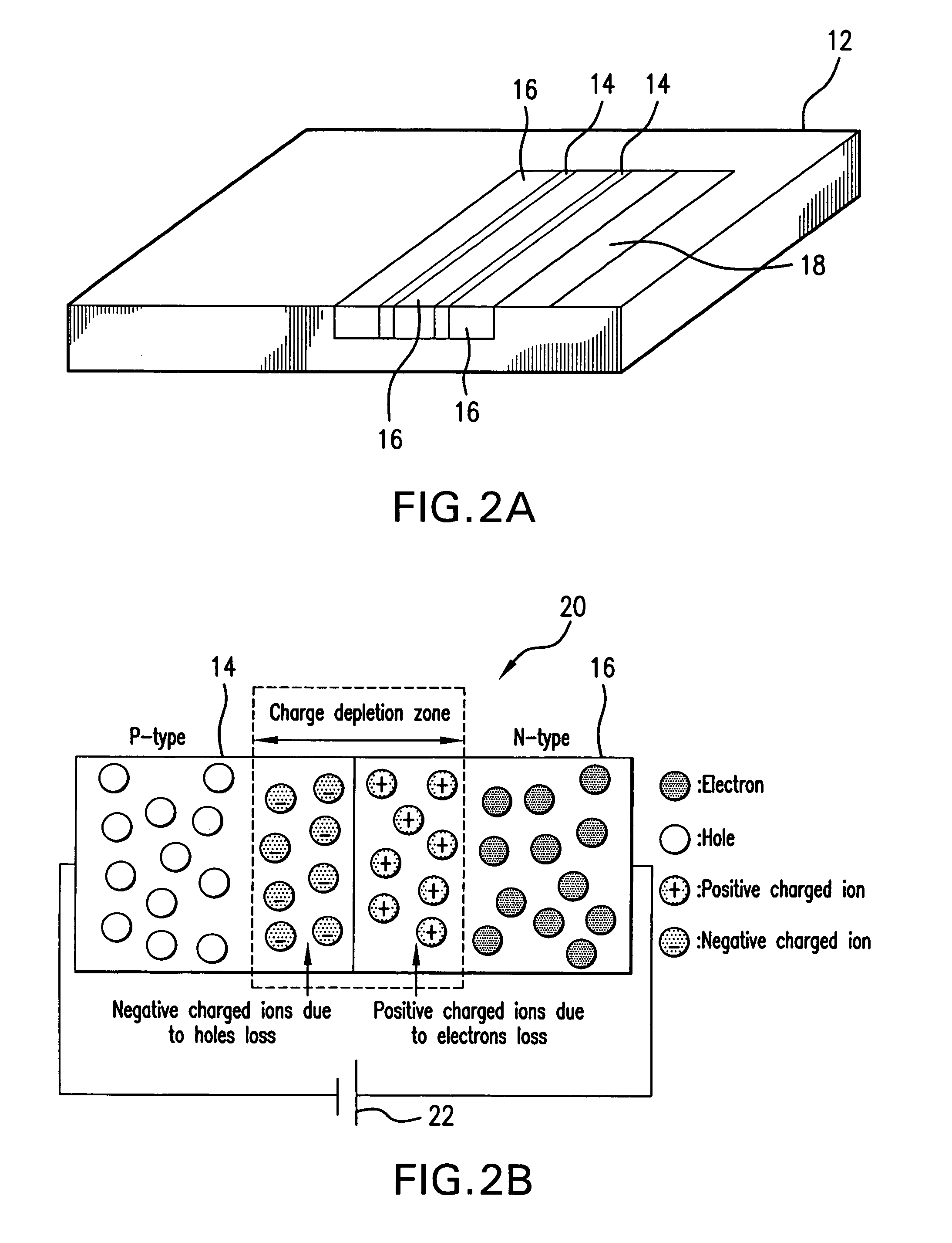
[0056]Referring to FIG. 1, a system 10 is shown for controllable nanoparticle deposition. A patterned substrate 12 shown in FIG. 2A, is patterned with an array of p-doped regions 14 and n-doped regions 16. The stripe-like pattern of p- and n-doped regions shown in FIG. 2A is only presented as an example. The p- and n-doped regions may be arrayed in any fashion to comply with an architecture of a nanoparticle-based device 18 to be fabricated on the substrate 12.

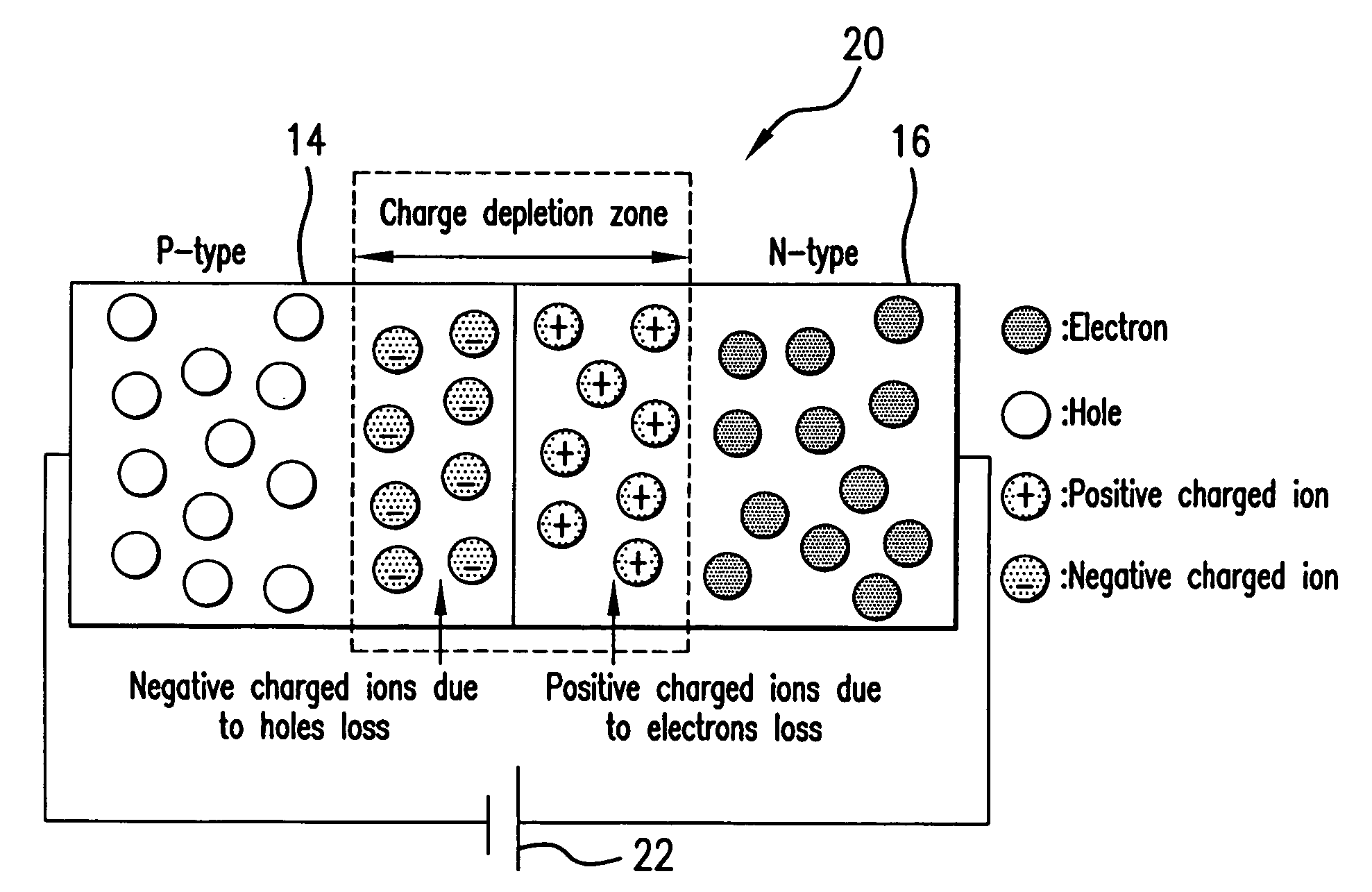
[0057]FIG. 2B illustrates in simplified form a p-n junction 20 formed on the substrate by respective p-doped region 14 and n-doped region 16. In the region where the p- and n-doped regions 14 and 16 are in contact, the electrons from the n-type region 16 diffuse towards the p-type region 14 and combine with the holes to form a charge depletion zone and the build-up of a net charge in each region.

[0058]When a reverse bias is applied to the p-n junction, the width of the charge depletion zone is increased, and an additional elec...


PUM

PropertyMeasurementUnit
temperatureaaaaaaaaaa
sizeaaaaaaaaaa
sizeaaaaaaaaaa

Abstract

In a method and system for controllable electrostatic-directed deposition of nanoparticles from the gas phase on a substrate patterned to have p-n junction(s), a bias electrical field is reversely applied to the p-n junction, so that uni-polarly charged nanoparticles are laterally confined on the substrate by a balance of electrostatic, van der Waals and image forces and are deposited on a respective p-doped or n-doped regions of the p-n junction when the applied electric field reaches a predetermined strength. The novel controllable deposition of nanoparticles employs commonly used substrate architectures for the patterning of an electric field attracting or repelling nanoparticles to the substrates and offers the opportunity to create a variety of sophisticated electric field patterns which may be used to direct particles with greater precision.

Description

REFERENCE TO RELATED APPLICATIONS[0001]This Utility Patent Application is based on Provisional Patent Application Ser. No. 60 / 656,454 filed 25 Feb. 2005.STATEMENT OF FEDERALLY SPONSORED RESEARCH / DEVELOPMENT[0002]This invention was made with Government Support under Contract Number H9823004C0448 awarded by the National Security Agency. The Government has certain rights in the invention.FIELD OF THE INVENTION[0003]This invention relates to manufacture of microelectronic devices. In particular, the present invention relates to the fabrication of nano-scale electronic systems.[0004]In overall concept, the present invention is related to a controllable deposition of nanoparticles on a substrate which is p-n junction patterned in compliance with the architecture of a nanoparticle-based device to be fabricated.[0005]Further, the present invention relates to positioning metal nanoparticles from the gas phase onto substrates by using electrostatic forces generated by a biased p-n junction cr...

Claims


Application Information

Patent Timeline
Patent Type & Authority Patents(United States)
IPC IPC(8): H01L21/31
CPCB82Y30/00C30B29/60C30B33/00Y10S438/962
Inventor ZACHARIAH, MICHAEL R.TSAI, DE-HAOPHANEUF, RAYMOND J.CORRIGAN, TIMOTHY D.KIM, SOO H.
Owner MARYLAND UNIV OF
Why Eureka
Try Eureka