Method for fine-pitch, low stress flip-chip interconnect

a flip-chip and interconnection technology, applied in the direction of adhesive types, solid-state devices, semiconductor devices, etc., can solve the problem that the pre-attach method is often used to make to-pad contacts with solderability problems

Active Publication Date: 2010-09-07
TEXAS INSTR INC
View PDF3 Cites 71 Cited by
  • Summary
  • Abstract
  • Description
  • Claims
  • Application Information

AI Technical Summary

Benefits of technology

[0010]Applicant solved the problem of inclusion of foreign particles in the member joints of two devices by mechanically vibrating one of the members with respect to the other member during the time period of the approach, until the contact areas of the device members touch. The vibrations preferably include displacements at right angles to the direction of the approach. The vibrations expel any foreign particles from the diminishing separation of the contact areas to enable surface contact of the two members without enclosing suspended solid particles or voids.
[0011]In one exemplary embodiment, the first member is a metallic bump attached to a semiconductor chip, the other member is a metallic pad of a substrate, and the viscous medium is a non-conductive paste (NCP) applied to the substrate before flip-chip attachment. The thermoset polymer precursor of the NCP includes 60 to 70% inorganic filler of silica particles between about 0.3 and 3 μm diameter. Alternatively, the NCP is pre-applied to the chip. The height of the chip bumps is in the range from 15 to 50 μm and the pitch center-to-center is less than 150 μm. The contact areas of the bumps and the surface of the pads may be covered with a cap of reflowable metal such as solder. During the time period it takes the bumps and pads to approach each other, the chip with the bumps vibrates relative to the substrate with the pads preferably so that the vibration includes displacements at right angles to the direction of the approach. The vibration frequency is preferably between 200 and 500 Hz, but may reach ultrasonic frequencies of more than 20 kHz dependent on the bump contact method. The back-and-forth or circular motion of the bumps expels compound along with any solid particle from the approaching contact areas of bumps and pads until the tip surfaces achieve intimate contact. When the contact areas include a cap of reflowable metal, the touching caps are molten and thus united. Applicant found that the vibrations allow the use of fine pitch solder-capped copper bumps of the chip (copper bump height in the range from 15 to 50 μm and bump pitch center-to-center less than 150 μm) and solder-capped copper pads of the substrate.
[0012]This method solves the contact reliability problem and enables the pre-attach method to be fully implemented to achieve underfilling of the stand-off between chip and substrate in fine-pitch devices.

Problems solved by technology

Applicant found that the bump-to-pad contacts made with the pre-attach method frequently show solderability issues during assembly.

Method used


Image

  • Method for fine-pitch, low stress flip-chip interconnect
  • Method for fine-pitch, low stress flip-chip interconnect

Examples


Embodiment Construction

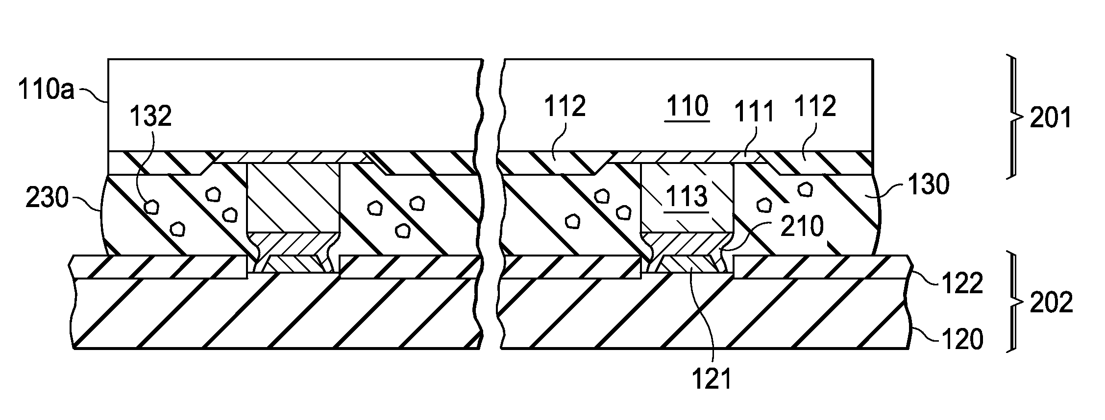
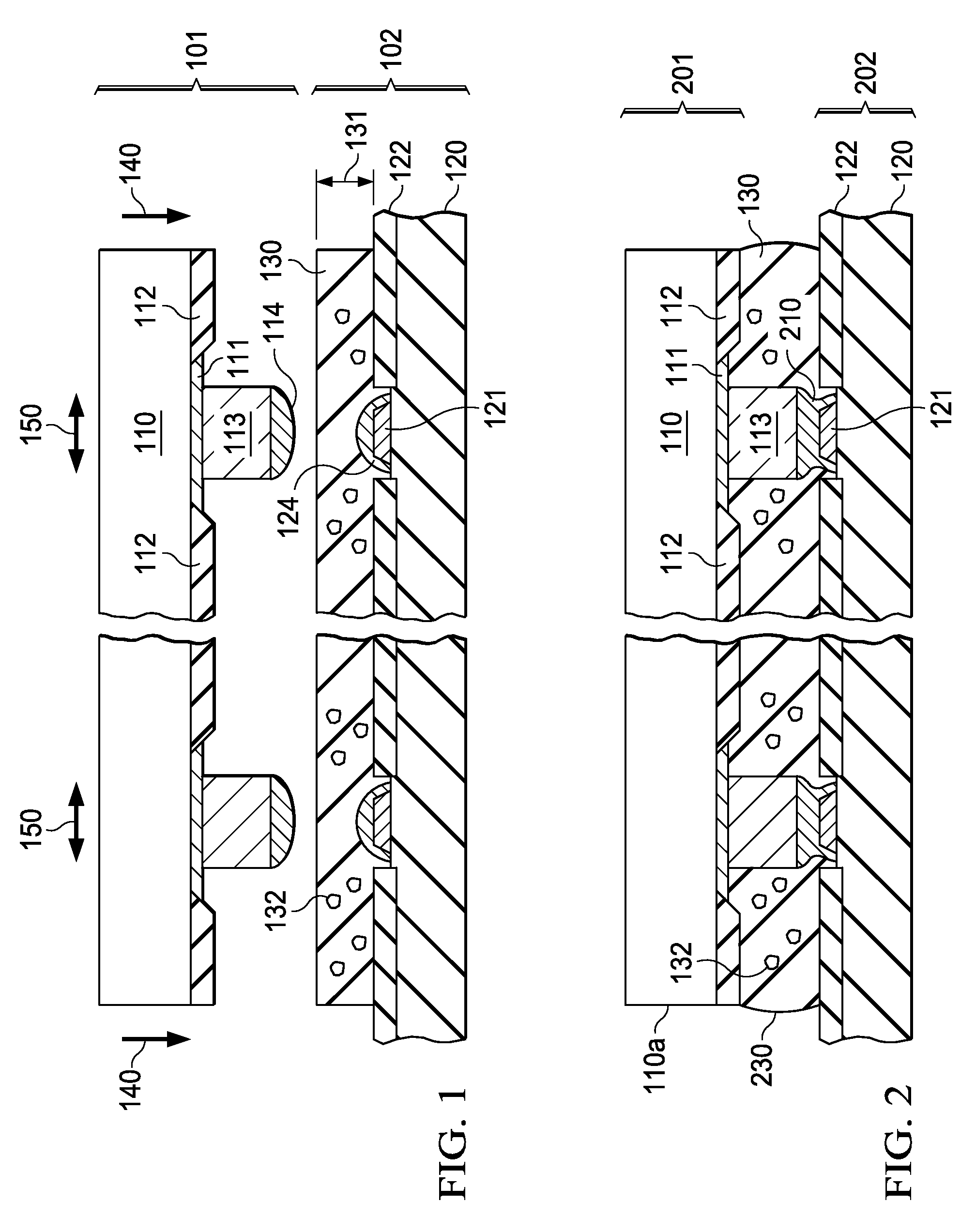
[0017]In FIG. 1, a first body 101 and a second body 102 are shown. First body 101 includes a base material 110, which by way of example is a semiconductor chip made of silicon, and at least one metallic terminal 111. As examples, terminals 111 are made of an aluminum alloy, copper, or a copper alloy. Terminals 111 are surrounded by a layer of insulating material 112, for instance a solder mask. Affixed to each terminal 111 is a first metallic member 113 made of a non-reflow metal or alloy, which is capped by a layer of reflow metal or alloy. In FIG. 1, first member 113 is shaped as a column or pillar with one end attached to terminals 111 and the opposite end having reflow metal 114. Pillar-shaped members 113 are frequently referred to as bumps or studs. The reflow metal 114 is exemplarily shaped as a half-dome because it has undergone one reflow process; reflow metal 114 represents the contact area of first member 113. (With gold to gold contacts, reflow metal may not be necessary)...


PUM

PropertyMeasurementUnit
heightaaaaaaaaaa
diameteraaaaaaaaaa
diameteraaaaaaaaaa

Abstract

Attaching a semiconductor chip to a substrate by applying mechanical vibrations (150) to a polymeric compound (130) and the contacting areas (114, 124) of a first (113) and a second (121) metallic member immersed in the compound, while the two metallic members approach (140) each other until they touch. The mechanical vibration causes displacements of the first member relative to the second member, and the vibration includes displacements (150) oriented at right angles to the direction (140) of the approach. The polymeric compound (130) includes a non-conductive adhesive resin paste (NCP) and filler particles; the paste is deposited before the attaching step. The first member (113) is affixed to the chip and the second member (121) to the substrate.

Description

FIELD OF THE INVENTION[0001]The present invention is related in general to the field of semiconductor devices and processes, and more specifically to the structure and fabrication method of flip-chip assembled fine-pitch bumped chips with stress-mitigating polymeric underfills.DESCRIPTION OF RELATED ART[0002]In a semiconductor device assembled by the flip-chip technology, the terminals of the semiconductor chip are connected to the contact pads of the substrate by metallic bumps; these bumps are solidly attached to the terminals as well as the pads, and conduct the electrical signals and power. After the assembly process, the chip is spaced apart from the substrate by a stand-off, with the metallic interconnections extending across the stand-off. As an approximate classification, interconnections with bumps of a diameter less than 100 μm and of a pitch center-to-center less than 150 μm are frequently called fine pitch interconnections.[0003]In many semiconductor devices with interco...

Claims


Application Information

Patent Timeline
Patent Type & Authority Patents(United States)
IPC IPC(8): H01L21/44
CPCC09J163/00H01L24/13H01L24/16H01L24/81H01L21/563H01L2924/1461H01L2224/13023H01L2224/1308H01L2224/13082H01L2224/13109H01L2224/13111H01L2224/13124H01L2224/13144H01L2224/13147H01L2224/73203H01L2224/81205H01L2224/81801H01L2224/83192H01L2924/01013H01L2924/01029H01L2924/01032H01L2924/01046H01L2924/01049H01L2924/01079H01L2924/14H01L2924/07802H01L2224/73204H01L2224/32225H01L2224/16225H01L2924/01087H01L2924/0105H01L2924/01047H01L2924/01033H01L2924/01019H01L2924/01006H01L2924/00013H01L2924/00014H01L2224/13099H01L2924/00H01L2224/05571H01L2224/05573
Inventor GERBER, MARK A
Owner TEXAS INSTR INC
Why Eureka
Try Eureka