Flash anneal for a PAI, NiSi process

a technology of nisi process and flash anneal, which is applied in the field of flash anneal for pai and nisi process, can solve the problems of stress related defects formed in the source/drain region, anneal process may degrade source/drain conductivity, and anneal process cannot cure this deficiency, so as to reduce the effect of pipe defects and spike structures, the effect of reducing the damag

Active Publication Date: 2010-09-14
TAIWAN SEMICON MFG CO LTD
View PDF32 Cites 2 Cited by
  • Summary
  • Abstract
  • Description
  • Claims
  • Application Information

AI Technical Summary

Benefits of technology

[0007]An advantage of a preferred embodiment of the present invention is that the effects of pipe defects and spike structures may be reduced or eliminated. A further advantage of a preferred embodiment of the present invention is that the conductivity of the source / drain region may be recovered, following the PAI process, by the flash anneal process.

Problems solved by technology

A disadvantage of the silicide process is the exacerbation of the stress related defects formed in the source / drain region.
While the use of a PAI process for relieving stress-retarded reaction and increasing nucleation density is known, there are disadvantages with the PAI process.
One such disadvantage of the PAI process is that the PAI process may degrade source / drain conductivity.
Typical anneal processes do not cure this deficiency.
Yet another disadvantage may be the degraded resistance in PMOS gated diodes, causing a degraded PMOS performance.

Method used


Image

  • Flash anneal for a PAI, NiSi process
  • Flash anneal for a PAI, NiSi process
  • Flash anneal for a PAI, NiSi process

Examples


Embodiment Construction

[0014]The making and using of the presently preferred embodiments are discussed in detail below. It should be appreciated, however, that the present invention provides many applicable inventive concepts that can be embodied in a wide variety of specific contexts. The specific embodiments discussed are merely illustrative of specific ways to make and use the invention, and do not limit the scope of the invention.

[0015]The present invention will be described with respect to preferred embodiments in a specific context, namely a drain region of a MOSFET. The invention may also be applied, however, to other areas of the MOSFET, including the source region.

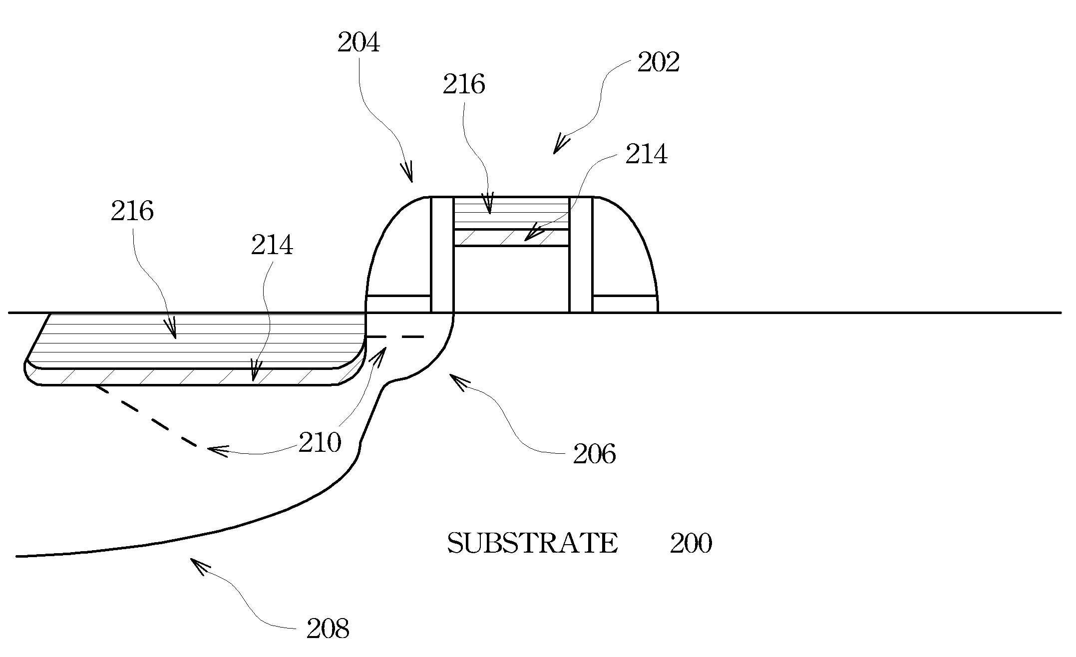
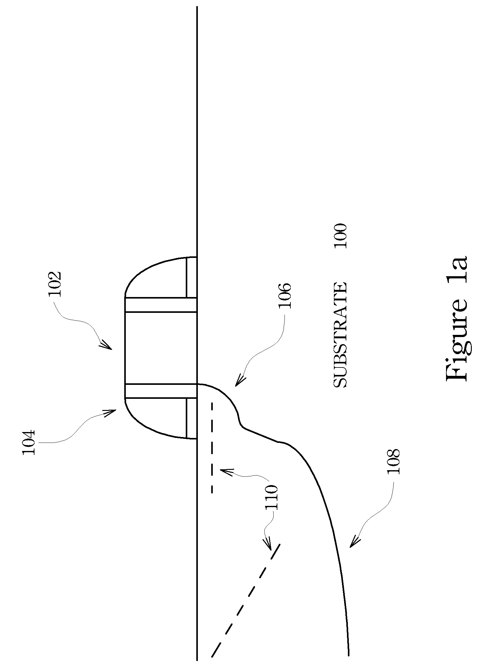
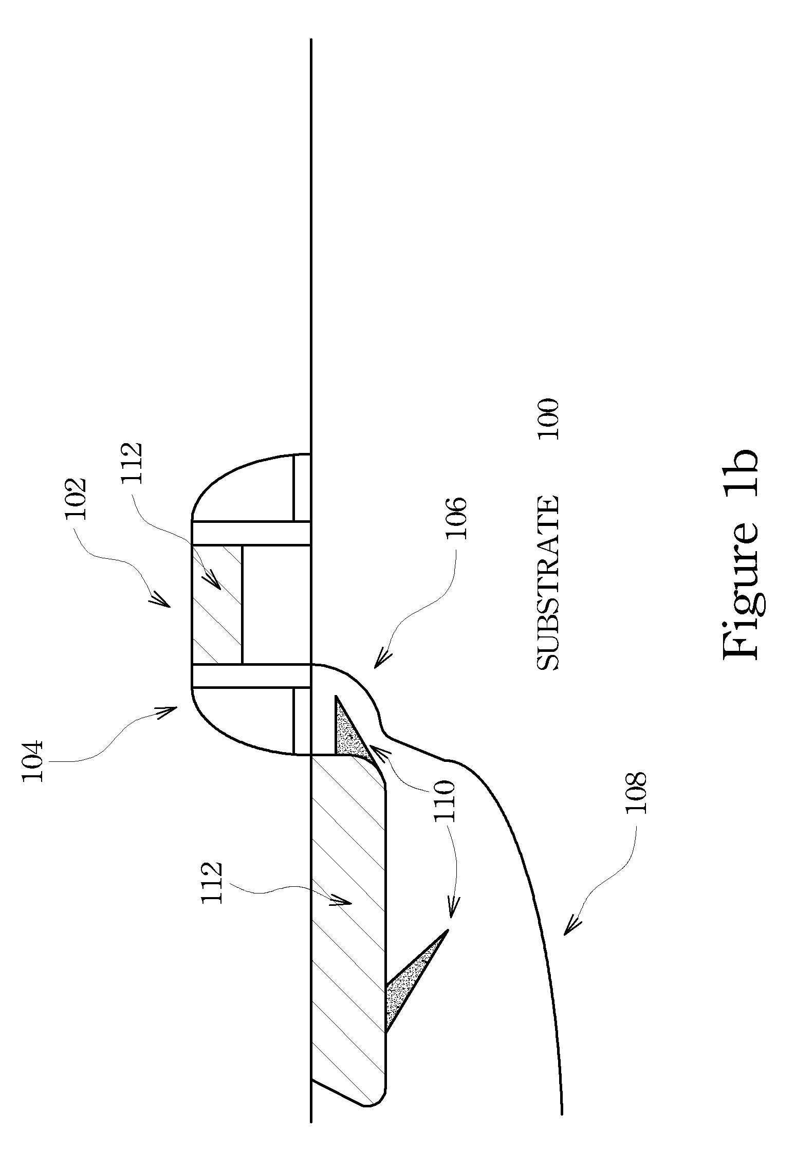
[0016]With reference now to FIG. 1a, a cross-sectional view of the un-repaired damage of a source / drain region of a prior art method is shown. Substrate 100 is a part of MOSFET shown with gate region 102. Gate region 102 comprises a gate electrode region of poly silicon and a thin gate oxide region (not explicitly shown). Spacer region ...


PUM


Abstract

A structure and a method for mitigation of the damage arising in the source / drain region of a MOSFET is presented. A substrate is provided having a gate structure comprising a gate oxide layer and a gate electrode layer, and a source and drain region into which impurity ions have been implanted. A PAI process generates an amorphous layer within the source and drain region. A metal is deposited and is reacted to create a silicide within the amorphous layer, without exacerbating existing defects. Conductivity of the source and drain region is then recovered by flash annealing the substrate.

Description

TECHNICAL FIELD[0001]The present invention relates generally to a system and method of manufacturing a semiconductor device, and more particularly to a system and method for mitigating source / drain defects in the semiconductor device by implementing pre-amorphous implant (PAI), NiSi silicidation and flash anneal processes.BACKGROUND[0002]Complementary metal oxide semiconductor (CMOS) field effect transistor (FET) technology involves the formation and utilization of n-channel FETs (NMOS) and p-channel FETs (PMOS) in combination (MOSFETs) to form low current, high performance integrated circuits.[0003]In sub-micron semiconductor technology, the use of self-aligned silicide processes has become widely accepted to minimize device series resistance. The silicide process is defined by introducing metal into silicon, which may overcome the high resistivity between metal and polysilicon gates and source / drain regions in MOSFETs. In the self-aligned silicide process, the polysilicon is depos...

Claims


Application Information

Patent Timeline
Patent Type & Authority Patents(United States)
IPC IPC(8): H01L21/04
CPCH01L21/26506H01L21/268H01L29/665H01L29/6659H01L29/7833H01L21/28052H01L21/324
Inventor LO, CHIA PINGLAI, JERRYWU, CHII-MINGWANG, MEI-YUNLIN, DA-WEN
Owner TAIWAN SEMICON MFG CO LTD
Why Eureka
Try Eureka