Method for forming wire portion of liquid crystal chromic device and liquid crystal chromic device

a wire portion technology, applied in the direction of door/window protective devices, instruments, chemistry apparatus and processes, etc., can solve the problems of increasing the size of the facility, the inability to remove the wire portion by solvent or other wet methods, and the increase in the cost of the facility, so as to improve the productivity and simplify the manufacturing process of the liquid crystal chromic device. , the effect of high reliability

Active Publication Date: 2020-02-13
LG CHEM LTD
View PDF5 Cites 0 Cited by
  • Summary
  • Abstract
  • Description
  • Claims
  • Application Information

AI Technical Summary

Benefits of technology

[0015]A method of forming a wire portion of a liquid crystal chromic device according to an embodiment of the present invention has an advantage that conductivity of a damaged transparent electrode can be recovered even by a relatively simple method.
[0016]Since the method of forming a wire portion of a liquid crystal chromic device according to the embodiment of the present invention can be performed according to a roll-to-roll continuous process, productivity can be improved.
[0017]In the method of forming a wire portion of a liquid crystal chromic device according to the embodiment of the present invention, since a masking step or a patterning step can be omitted in advance and an appropriate wire portion can be formed according to a size of a product in a postprocess, a liquid crystal chromic device manufacturing process is simplified.
[0018]In the method of forming a wire portion of a liquid crystal chromic device according to the embodiment of the present invention, the wire portion can be formed with high reliability while using a low-cost laser facility.

Problems solved by technology

For example, a liquid crystal alignment layer such as reactive mesogen is coated over the entire conductive film substrate in a UV curing scheme and in this case, a wire portion cannot be removed by using a solvent or other wet method.
Meanwhile, the patterning process described above is troublesome in that overlay accuracy of upper layers such as the conductive layer and the liquid crystal alignment layer on the substrate needs to be ensured in the process and has a disadvantage that cost of a facility increases in an increase in size.

Method used


Image

  • Method for forming wire portion of liquid crystal chromic device and liquid crystal chromic device
  • Method for forming wire portion of liquid crystal chromic device and liquid crystal chromic device
  • Method for forming wire portion of liquid crystal chromic device and liquid crystal chromic device

Examples


examples 1 to 10

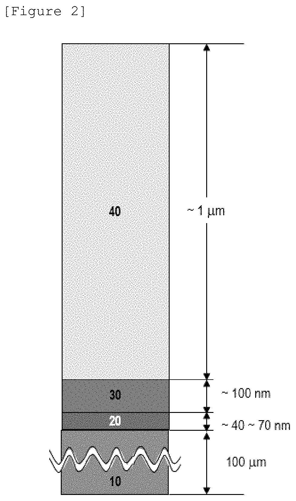
[0135]A COP substrate having a thickness of about 40 μm, a transparent electrode including ITO having a thickness of about 40 nm, an alignment film having a thickness of about 80 nm including a photo-alignment compound (LG CHEM) based on a norbornene resin including a cinnamate functional group, and a liquid crystal alignment film having a thickness of about 1 μm including a reactive mesogen (RMM141C, MERCK) are sequentially provided to prepare a liquid crystal chromic device (1,000 mm×500 mm).

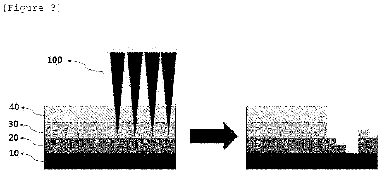
[0136]A fiber laser (G4, SPI, F-theta lens scanner) having an average output of about 50 W and a wavelength of 1064 nm was irradiated onto the liquid crystal chromic device at a repetition rate of 100 kHz, an output ratio of 45% and an irradiation speed of 2 m / s and irradiated in areas having a size of 10 mm×10 mm (width×length) on the liquid crystal alignment film by adjusting an irradiation interval as shown in Table 1 below, respectively, to form etching lines in the liquid crystal chromic ...

examples 11 to 19

[0141]As Examples for a liquid crystal chromic device for a sunroof, a COP substrate having a thickness of about 40 μm, a transparent electrode including ITO having a thickness of about 40 nm, an alignment film having a thickness of about 100 nm including a photo-alignment compound (LG CHEM) based on a norbornene resin including a cinnamate functional group, and a liquid crystal alignment film having a thickness of about 1.2 including a reactive mesogen (RMM141C, MERCK) are sequentially provided to prepare a liquid crystal chromic device.

[0142]In the liquid crystal chromic device, a Galvano Scanner based infrared laser with an average output of about 50 W and a wavelength of 1064 nm was irradiated on the liquid crystal alignment film with respect to a laser irradiation area of 80 mm×5 mm (width×length) at a repetition rate of 100 kHz and an irradiation speed of 2.5 m / s by adjusting the irradiation interval as shown in Table 2 below to form etching lines in the liquid crystal chromic...

experimental example 3

[Experimental Example 3]—Climate Change Test

[0171]A process in which the liquid crystal chromic device provided with the wire portion according to Examples 11 to 19 was heated to a temperature of about 90° C. from a temperature of −40° C. at a speed of about 1° C. / min, maintained for 4 hours, and then lowered to about −40° C. from about 90° C. at a speed of about 1° C. / min, and maintained for 4 hours was repeated ten times to perform a climate evaluation. A graph of temperature and humidity conditions at the time of such a climate change test is shown in FIG. 13.

[0172]FIG. 14 illustrates a photograph of an appearance after evaluating a climate change test of the liquid crystal chromic device provided with the wire portion according to Examples 11 to 19, particularly, a photograph of an appearance after adjusting output ratios of the laser during laser irradiation to 25%, 30%, 35% and 40% with respect to the average output, respectively, and evaluating a climate change test of the li...


PUM

PropertyMeasurementUnit
thicknessaaaaaaaaaa
sizeaaaaaaaaaa
thicknessaaaaaaaaaa

Abstract

A method for forming a wire portion of a liquid crystal chromic device. The method includes: a) preparing a liquid crystal chromic device by forming a transparent electrode on a substrate, and forming an alignment film on the transparent electrode; b) forming two or more etching lines spaced apart by a constant interval by irradiating the alignment film with a laser; and c) applying a conductive paste to a valley region of each of the two or more etching lines. The liquid crystal chromic device includes: a substrate; a transparent electrode provided on the substrate; an alignment film provided on the transparent electrode; and two or more etching lines provided on the alignment film. The two or more etching lines are spaced apart by a constant interval, and a valley region of each of the two or more etching lines is coated with a conductive paste.

Description

CROSS-REFERENCE TO RELATED APPLICATION[0001]This application is the national stage of international Application No. PCT / KR2017 / 015542 filed Dec. 27, 2017, which claims priority to, and the benefit of, Korean Patent Application No. 10-2016-0180381 filed in the Korean Intellectual Property Office on Dec. 27, 2016, the entire contents of which are incorporated herein by reference.TECHNICAL FIELD[0002]The specification relates to a method for forming a wire portion of a liquid crystal chromic device and a liquid crystal chromic device.BACKGROUND ART[0003]With the rapid development of flexible electronic devices, the importance of large-area patterning processes with high productivity has been raised. Further, in implementation of the flexible electronic devices, not only a short circuit of a conductive layer for electrode formation or wiring but also a process for implementing and structuring a conductive film is required.[0004]In the development of transmission variable liquid crystal ...

Claims


Application Information

Patent Timeline
Patent Type & Authority Applications(United States)
IPC IPC(8): G02F1/1362G02F1/1337
CPCG02F1/133711G02F1/136286G02F2001/136295H01S3/067C09K19/56G02F1/1337G02F1/155G02F1/163H01B1/22H01B1/24E06B9/24G02F1/13306G02F1/1333G02F2202/16G02F2203/48E06B2009/2464G02F1/133726G02F1/133723G02F1/133788G02F1/136295
Inventor PARK, JEONG HOSHIN, BU GONHER, EUN KYU
Owner LG CHEM LTD
Why Eureka
Try Eureka