
Solid-state imaging device and method for driving the same

a solid-state imaging and imaging device technology, applied in semiconductor/solid-state device manufacturing, semiconductor devices, electrical devices, etc., can solve problems such as shading and irregular brightness of output images, and achieve the effect of reducing the size of the imaging apparatus comprising the solid-state imaging device and high-quality video

Active Publication Date: 2010-09-21
PANASONIC SEMICON SOLUTIONS CO LTD
View PDF10 Cites 20 Cited by
  • Summary
  • Abstract
  • Description
  • Claims
  • Application Information

AI Technical Summary

Benefits of technology

The present invention provides a solid-state imaging device that suppresses the occurrence of shading, which refers to irregularity in brightness of an output image caused by variations in capacitance and photoelectric conversion characteristics. The device includes a pixel array with photodiodes, floating diffusions, transfer transistors, amplifying transistors, and vertical signal lines. The layout of the wiring layers and the arrangement of the cells in the pixel array are designed to improve oblique incident light characteristics and suppress shading. Additionally, the device includes a light-shielded pixel region to improve video quality. The technical effects of the invention include improved image quality and reduced shading in the output image.

Problems solved by technology

Therefore, in the conventional solid-state imaging device, light enters in laterally different manners, so that irregularity may occur in the brightness of an output image.
Such a defect causes a significant problem, particularly in applications which require high image quality.
In the solid-state imaging devices of FIGS. 32 and 33, a capacitance between an FD and a metal wire in the pixel array varies due to shrink, likely leading to the occurrence of shading.

Method used


Image

  • Solid-state imaging device and method for driving the same
  • Solid-state imaging device and method for driving the same
  • Solid-state imaging device and method for driving the same

Examples


first embodiment

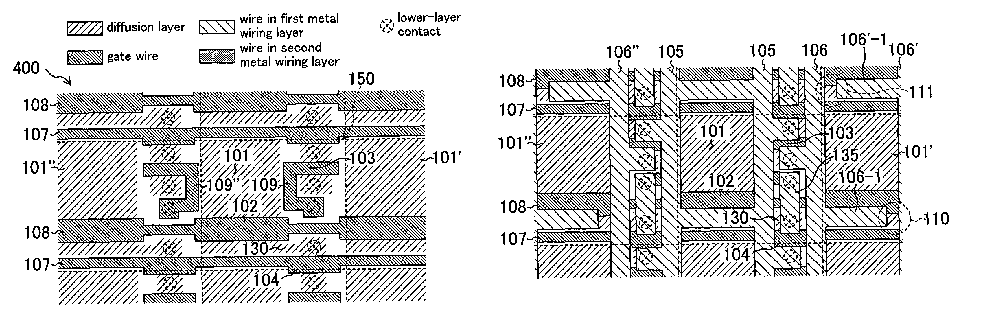
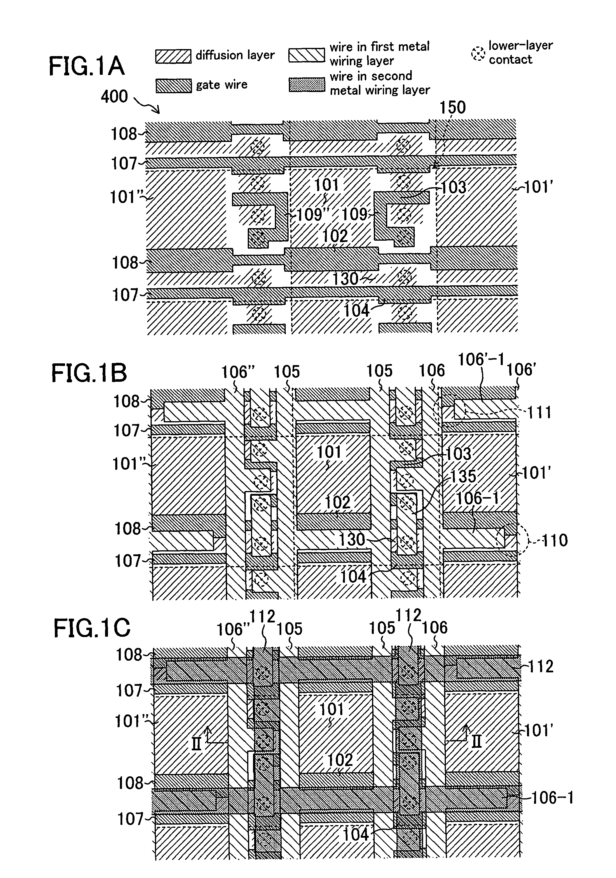
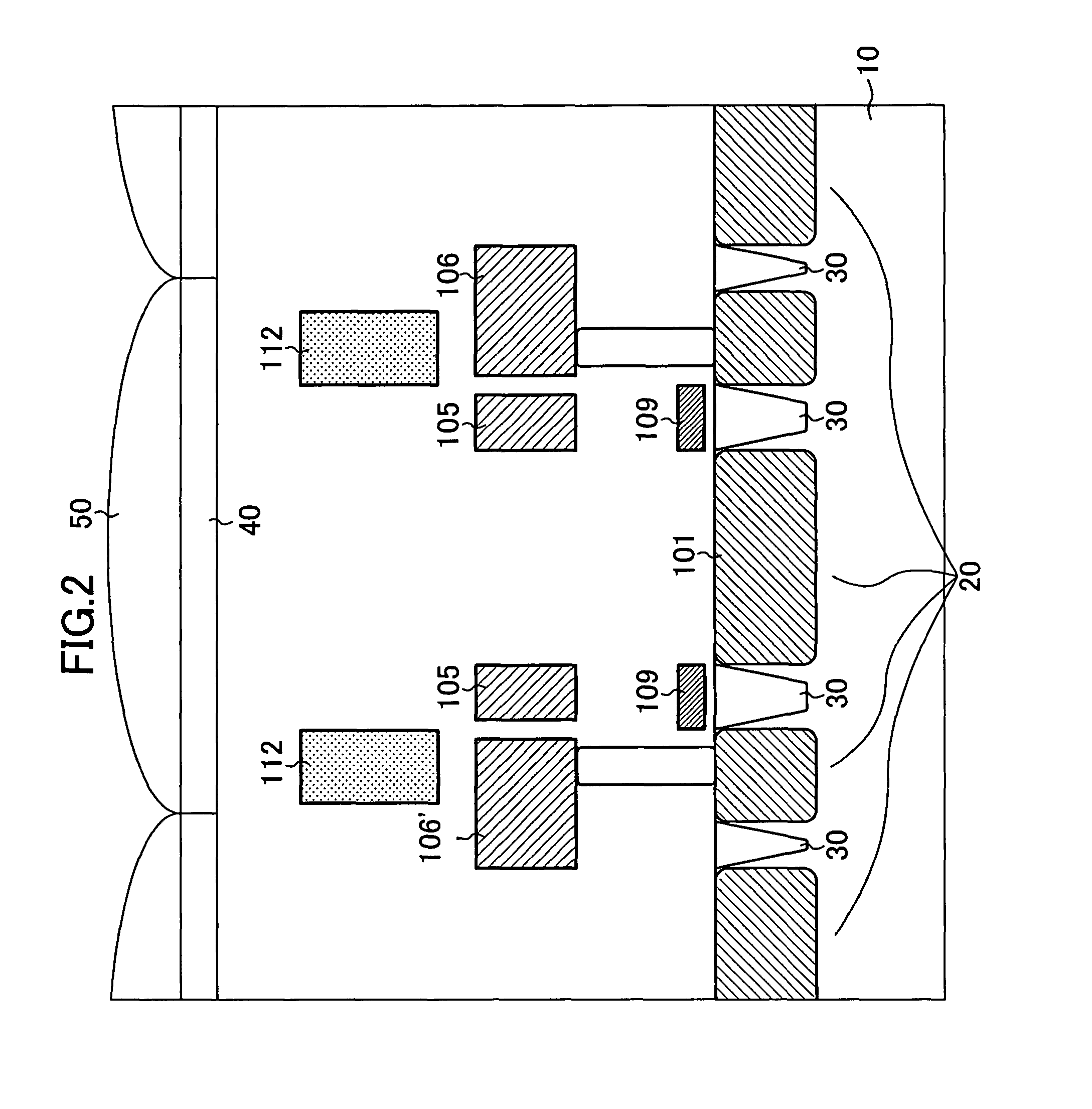
[0069]FIGS. 1A to 1C are plan views illustrating a layout of a pixel array of a solid-state imaging device (MOS solid-state imaging device) according to a first embodiment of the present invention. FIG. 1A illustrates, in the pixel array, a polysilicon wiring layer, and contacts (lower-layer contacts) connecting a diffusion layer or polysilicon wires formed on a semiconductor substrate, and wires in a first metal wiring layer. FIG. 1B illustrates wires formed in the first metal wiring layer in addition to the configuration of FIG. 1A. FIG. 1C further illustrates wires formed in a second metal wiring layer in addition to the configuration of FIG. 1B. In FIGS. 1A to 1C, each portion surrounded by a dashed line is a cell 150. When one photodiode is provided in each cell as in the solid-state imaging device of this embodiment, the cell is generally called a “pixel cell”. FIG. 2 is a cross-sectional view of the solid-state imaging device of the first embodiment, taken along line II-II of...

second embodiment

[0106]FIGS. 9A to 9C are plan views illustrating a layout of a pixel array of a solid-state imaging device according to a second embodiment of the present invention. FIG. 9A illustrates a polysilicon wiring layer, and contacts connecting a diffusion layer or polysilicon wires formed on a semiconductor substrate and wires formed in a first metal wiring layer, in a pixel array. FIG. 9B illustrates the wires formed in the first metal wiring layer, and contacts (vias) connecting the first metal wiring layer and a second metal wiring layer in addition to the configuration of FIG. 9A. FIG. 9C illustrates wires formed in the second metal wiring layer in addition to the configuration of FIG. 9B. FIG. 10 is a cross-sectional view of the solid-state imaging device of the second embodiment, taken along line X-X of FIGS. 9A to 9C.

[0107]The solid-state imaging device of this embodiment is different from the solid-state imaging device of the first embodiment in a portion of the wire layout. Speci...

third embodiment

[0116]FIGS. 11A to 11C are plan views illustrating a layout of a pixel array of a solid-state imaging device according to a third embodiment of the present invention. FIG. 11A illustrates a polysilicon wiring layer, and contacts connecting a diffusion layer or polysilicon wires formed on a semiconductor substrate and wires in a first metal wiring layer, in the pixel array. FIG. 11B illustrates wires formed in the first metal wiring layer, and contacts connecting the first metal wiring layer and a second metal wiring layer, in addition to the configuration of FIG. 11A. FIG. 11C further illustrates wires formed in the second metal wiring layer in addition to the configuration of FIG. 11B.

[0117]The solid-state imaging device of this embodiment is different from the solid-state imaging devices of the first and second embodiments in a portion of the wire layout. Specifically, in the solid-state imaging device of this embodiment, each cell 350 comprises: a photodiode 301; an FD 330; a tra...


PUM


Abstract

A pixel array is provided in which cells are arranged in a matrix. Each cell includes a photodiode, an FD, a transfer transistor, a reset transistor, an amplifying transistor having a gate electrode connected to the FD, a drain connected to a power supply line, and a source connected to a vertical signal line, and an FD wire. The FD wire is provided in a first wiring line, and the vertical signal line is provided in a second wiring line positioned over the first wiring layer. Since the potential of the FD wire follows the potential of the vertical signal line, it is possible to suppress a variation in capacitance occurring in the FD when a position of the vertical signal is shifted, depending on a position of the cell.

Description

BACKGROUND OF THE INVENTION[0001]1. Field of the Invention[0002]The present invention relates to a MOS solid-state imaging device for use in a digital camera or the like, and a method for driving the same.[0003]2. Description of the Related Art[0004]In recent years, as the function, miniaturization level and the like of imaging elements are improved, solid-state imaging devices (imaging chips) including the imaging element are employed within an increasing range of applications. For example, while a solid-state imaging device having a miniaturized imaging element is incorporated into a mobile telephone or the like, a solid-state imaging device adapted to improve image quality is used in a high-grade digital camera or the like, such as a single-lens reflex camera or the like. Solid-state imaging devices used in any products have basic common features, and each comprise a pixel array of a plurality of cells which receive external light.[0005]FIGS. 27A to 27C are plan views illustratin...

Claims


Application Information

Patent Timeline
Patent Type & Authority Patents(United States)
IPC IPC(8): H01L31/042H04N25/00
CPCH01L27/14603H01L27/14636H04N25/60H04N25/76
Inventor OHTSUKI, HIROHISAKATSUNO, MOTONARIMIYAGAWA, RYOHEI
Owner PANASONIC SEMICON SOLUTIONS CO LTD
Learn More