Dispersion compensating circuits for optical transmission system

a technology of optical transmission system and compensating circuit, which is applied in the direction of wave amplification device, electrical apparatus, laser details, etc., can solve the problems of high cost of dcf, serious second-order distortion, and communication signal distortion, and achieve linear delay time compensation, high degree of accuracy, and easy compensation of different fiber lengths

US7809282B2Inactive Publication Date: 2010-10-05GOOGLE TECH HLDG LLC
23 Cites 6 Cited by

Patent Information

Authority / Receiving Office
US · United States
Patent Type
Patents(United States)
Current Assignee / Owner
Publication Date
2010-10-05
Estimated Expiration
Not applicable · inactive patent

Smart Images

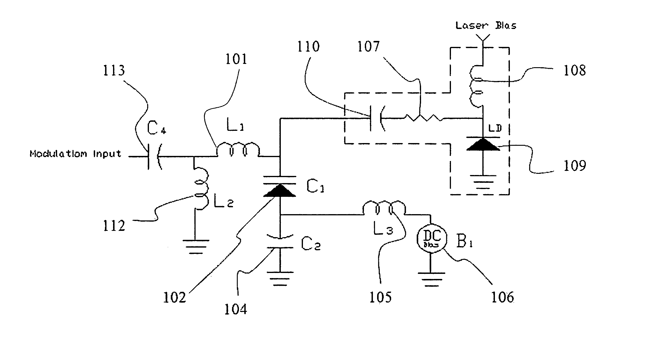
  • Figure 1
    Figure 1
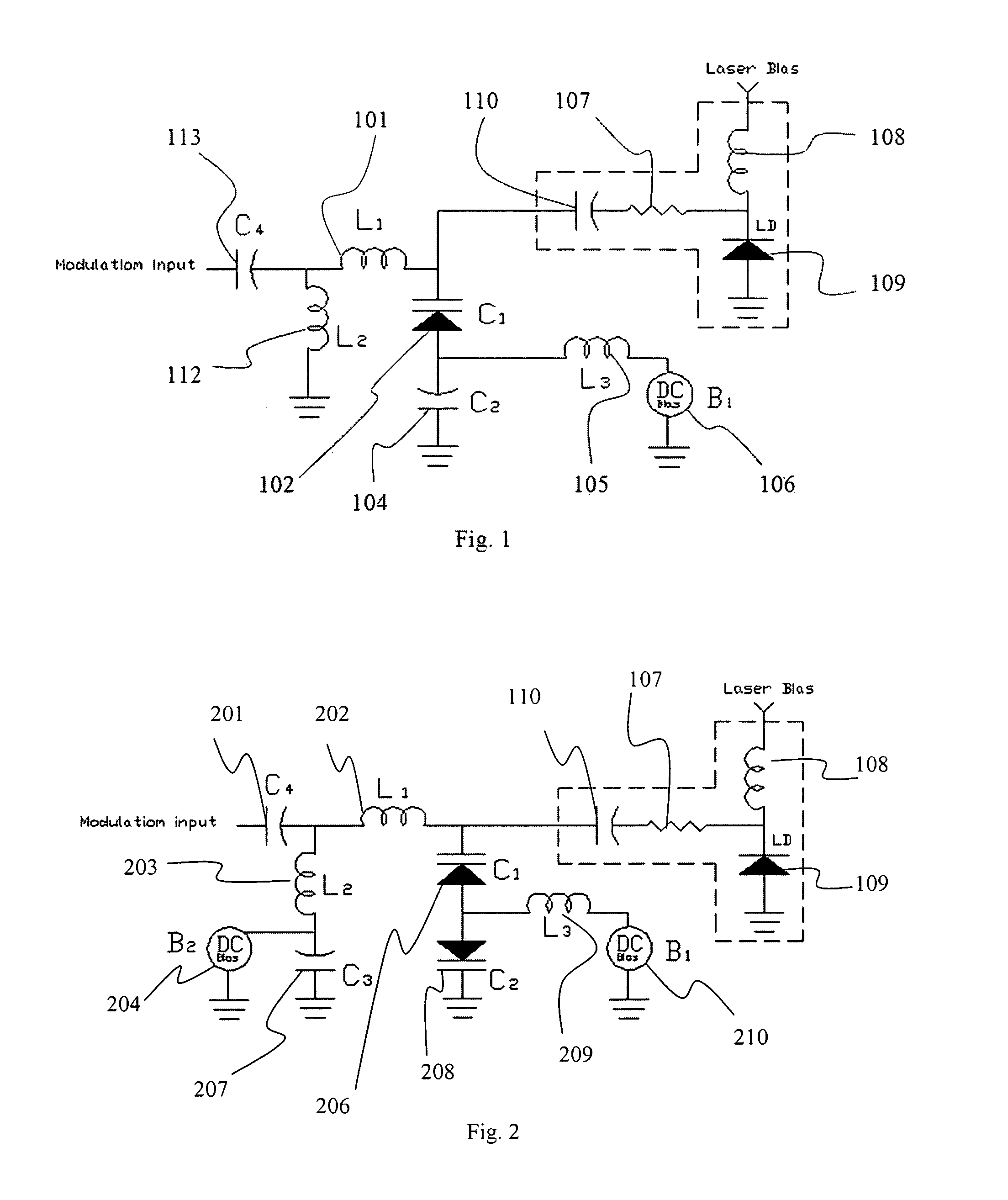
  • Figure 2
    Figure 2
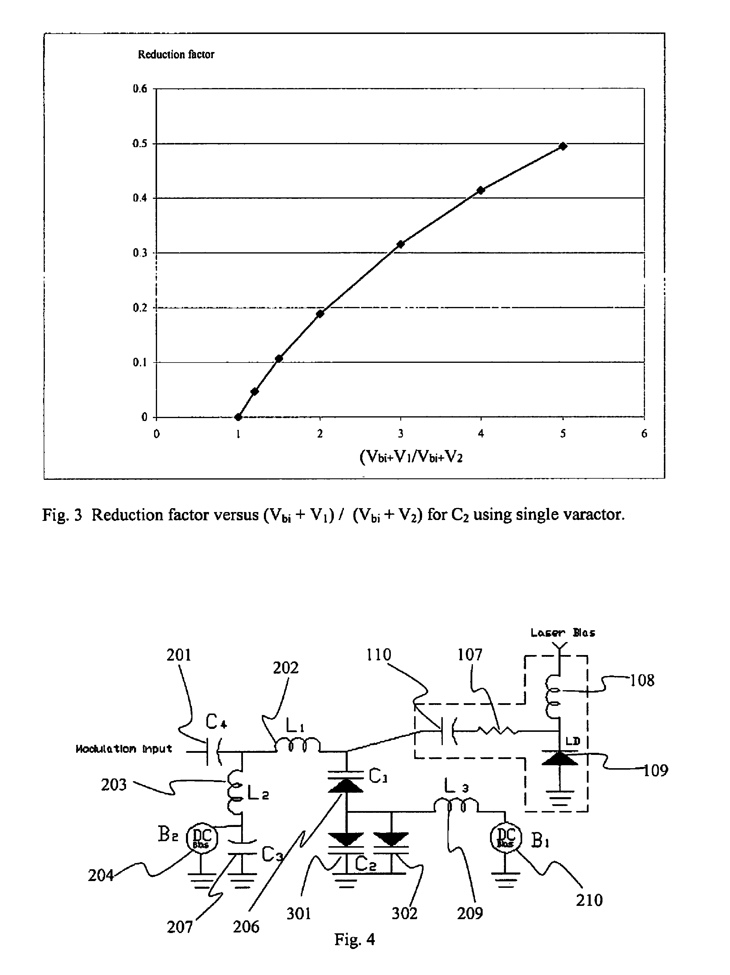
  • Figure 3
    Figure 3
Patent Text Reader

Abstract

Improved dispersion compensating circuits for optical transmission systems are disclosed. According to the improved method, there is provided a compensation circuit comprising a varactor diode network. The network is preferably inserted between a source of laser modulating signal and the laser. A low pass filter constructs the network. The network preferably includes an inductance and a combined circuit, which includes varactors. The network preferably provides an amplitude dependent delay of the modulating signal applied to the laser. In a first embodiment, a fixed capacitor is in series with a varactor and connected to a DC bias through inductor. In a second embodiment, second varactor is in series with varactor instead with an opposite polarity of a fixed capacitor as used in the first embodiment. In a third embodiment, two varactors 301 and 302 are used in place of the fixed capacitor in parallel.
Need to check novelty before this filing date? Find Prior Art

Description

FIELD OF THE INVENTION

[0001] The present invention relates to optical transmission systems and dispersion compensating circuit associated with optical transmission systems. In particular the present invention relates to delay caused distortion compensating circuits associated with optical transmission systems.BACKGROUND OF THE INVENTION

[0002] Optical transmission systems are widely used to transmit data on a broadband network. In a typical optical transmission system, a laser provides an optical signal at a predetermined frequency which is typically modulated to provide an optical transmission data signal.

[0003] In Broadband Passive Optical Network (B-PON) applications, a 1550 nm optical signal is assigned for video signal transmission. An externally modulated laser transmitter is typically used for optical signals because an externally modulated laser transmitter has much lower chirp than a directly modulated laser transmitter. A directly modulated laser transmitter, especially a high...

Examples

Embodiment Construction

[0026]According to the improved method, there is provided a compensation circuit comprising a varactor diode network. The network is preferably inserted between a source of laser modulating signal and the laser. A low pass filter constructs the network. The network preferably includes an inductance and a combined circuit, which includes varactors. The network preferably provides an amplitude dependent delay of the modulating signal applied to the laser.

[0027]The capacity of a varactor at any voltage can be expressed by

C(V)=Cj0(1−V / Vbi)−γ=Cj1(Vbi−V)−γ  (1)

Where Cj1=Cj0(Vbi)−γ  (2)

[0028]Here C(V) is the varactor capacity at any instant voltage. Cj0 is the varactor capacity at zero voltage. γ is a parameter depending on the varactor doping profile. For example, γ=0.5 for an abrupt junction, γ=1 for a hyper-abrupt junction.

[0029]The group delay for the delay-compensating network may be given by

Tgd=(L1*C(V))1 / 2  (3)

δTgd=(½)*(δC / C)*Tgd  (4)

[0030]Here Tgd is the varactor network delay time...