Dispersion Compensating Varactor Circuit

a varactor circuit and dispersion compensation technology, applied in process and machine control, semiconductor lasers, instruments, etc., can solve the problems of dcf cost, communication signal distortion, and serious second order distortion, and achieve linear delay time compensation, large amplitude rf driving voltage, and easy adjustment

Inactive Publication Date: 2009-10-01
GOOGLE TECH HLDG LLC
View PDF6 Cites 21 Cited by
  • Summary
  • Abstract
  • Description
  • Claims
  • Application Information

AI Technical Summary

Benefits of technology

[0024]The present invention offers compensation methods for the nonlinear varactor capacitance change thereby permitting larger amplitude RF driving voltage. Thus, linearized delay time compensation can be obtained even with large RF drive voltage. This

Problems solved by technology

The large total laser chirp helps improve the Stimulated Brillouin Scattering (SBS) suppression optical power level, but as a result of fiber dispersion, introduces serious second order distortions, such as Composite Second Order (CSO) distortion.
When the chirped optical frequencies pass through a fiber, different optical wavelengths propagate at different group velocities, which causes delay dispersion at the receiving end and often causes di

Method used


Image

  • Dispersion Compensating Varactor Circuit
  • Dispersion Compensating Varactor Circuit
  • Dispersion Compensating Varactor Circuit

Examples


Embodiment Construction

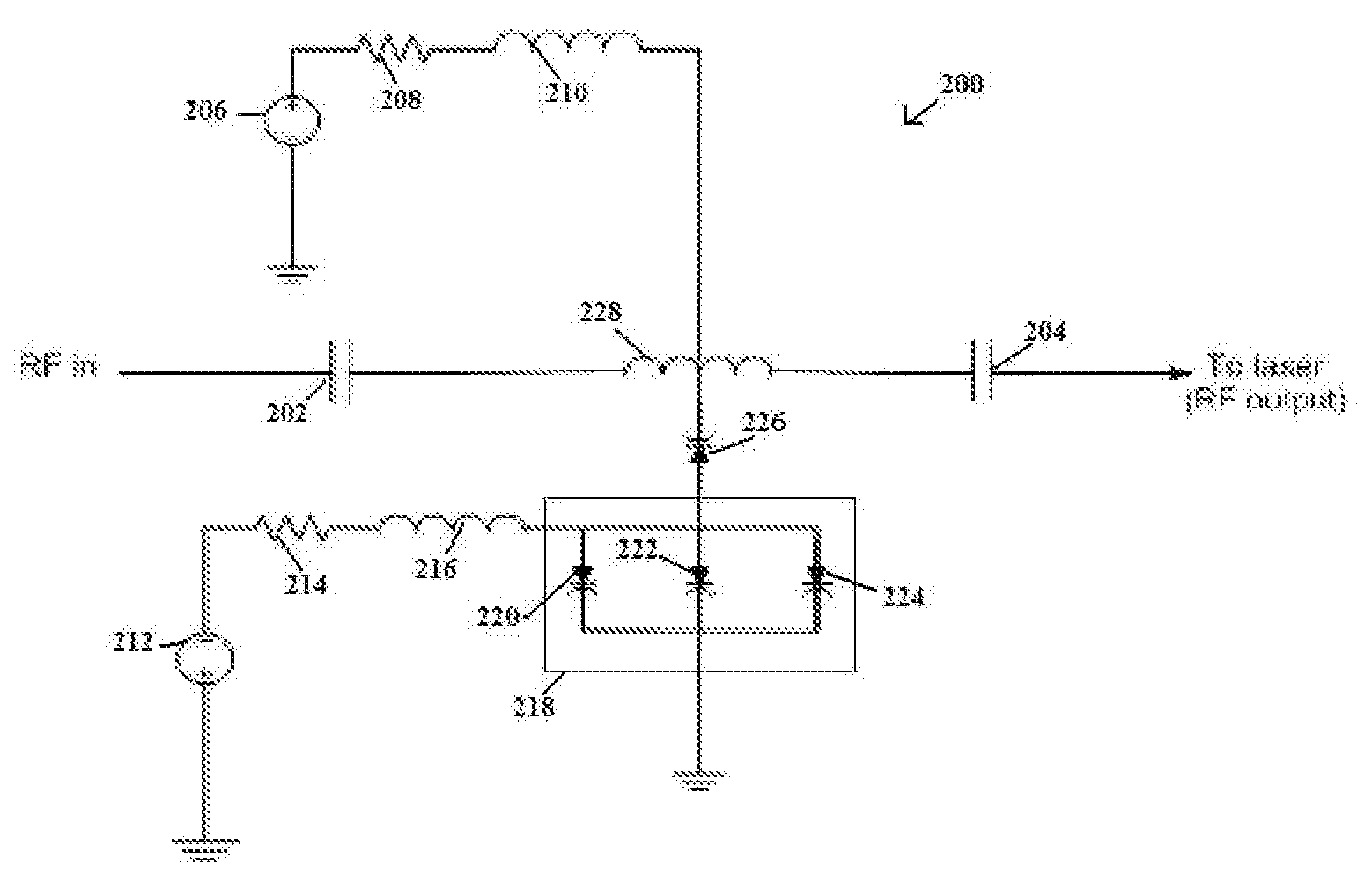
[0032]The capacitance of a varactor at any voltage can be expressed by:

C(V)=Cj0(1−V / Vbi)−γ=Cj1(Vbi−V)−γ,  (1)

where Cj1=Cj0(Vbi)−γ.  (2)

[0033]Here C(V) is the varactor capacitance at any instant voltage. Cj0 is the varactor capacitance measured at zero voltage. Vbi is the varactor junction voltage. γ is the varactor doping profile parameter. For example, γ=0.5 for an abrupt junction, γ=1 for a hyper-abrupt junction.

[0034]The group delay for the delay-compensating network may be given by:

Tgd=(L1*C(V))1 / 2;  (3)

δTgd=(½)*(δC / C)*Tgd.  (4)

[0035]Here Tgd is the varactor network delay time, L1 is the inductance in the delay network, and δTgd is the delay time difference selected for the dispersion compensation.

[0036]The RF signal swing at the varactor causes the capacitance of the varactor to change. δC / C is the varactor capacitance change due to the RF voltage swing. The dispersion compensation ability is proportional to the varactor capacitance change δC / C caused by the RF voltage swing.

[0...


PUM


Abstract

Improved dispersion compensating circuits for optical transmission systems are disclosed. According to the improved method, there is provided a compensation circuit comprising a varactor diode network. The network is preferably inserted between a source of laser modulating signal and the laser. A low-pass filter or all pass filter constructs the network. The network preferably includes an inductor or inductors and a combined circuit, which includes varactors. The network preferably provides an amplitude dependent delay of the modulating signal applied to the laser or to the optical receiver as post dispersion correction circuitry. In a first embodiment, a fixed capacitor is in series with a varactor and connected to a DC bias through inductor. Additional embodiments, using multiple varactors in different circuit configurations, with particular advantages for various applications identified.

Description

BACKGROUND[0001]1. Field of the Invention[0002]The present invention relates to fiber optic transmission systems and dispersion compensating circuits associated with optical transmission systems. In particular the present invention compensates for the laser chirp and chromatic dispersion distortions to enable effective broadband transmission and extended fiber link reach.[0003]2. Background of the Invention[0004]Optical transmission systems are widely used to transmit data on a broadband network. In a typical optical transmission system, a laser provides an optical signal at a predetermined frequency, which is typically modulated to provide an optical transmission data signal.[0005]In Broadband Passive Optical Network (B-PON) or Gigabit-Passive Optical Network (G-PON) applications, the longest distance is 20 km. So the dispersion compensation needs only to be adequate for fiber lengths up to 20 km.[0006]In Hybrid Fiber Coaxial (HFC) networks and narrowcast overlay digital applicatio...

Claims


Application Information

Patent Timeline
IPC IPC(8): H04B10/18H01S3/00
CPCH04B10/6972H01S5/0427
Inventor KHALOUF, IHABMEIER, RICHARDZHOU, SHUTONG
Owner GOOGLE TECH HLDG LLC
Why Eureka
Try Eureka