Plasma processing method

a plasma processing and plasma technology, applied in the field of capacitively coupled plasma processing apparatus, can solve the problems of difficult fine adjustment, damage to the variable condenser, and insufficient effect,

Active Publication Date: 2015-09-17
TOKYO ELECTRON LTD
View PDF4 Cites 17 Cited by
  • Summary
  • Abstract
  • Description
  • Claims
  • Application Information

AI Technical Summary

Benefits of technology

[0016]According to the plasma processing method of the present disclosure, by such the configuration and the operation, in the capacitively coupled plasma processing apparatus that distributes and supplies the high-frequency power to the inner upper electrode and the outer upper electrode disposed to face the lower electrode on which the substrate is placed, the function can be remarkably improved as the adjustment knob for controlling the plasma density distribution characteristic of the variable condenser provided to control the outer / inner power distribution ratio or the in-plane profile of the process characteristic.

Problems solved by technology

Since an outer / inner power distribution ratio is significantly changed at a rapid change rate (slope) around the resonance point even though the capacitance of the variable condenser is slightly changed, fine adjustment becomes difficult, and large current flows in the closed circuit, which may result in damage of the variable condenser.
However, since a variable range or a dynamic range of the outer / inner power distribution ratio is small in practice, an effect is slightly insufficient as an adjustment knob for controlling a plasma density distribution or a profile of a process characteristic in the radial direction.

Method used


Image

  • Plasma processing method
  • Plasma processing method
  • Plasma processing method

Examples


example 1

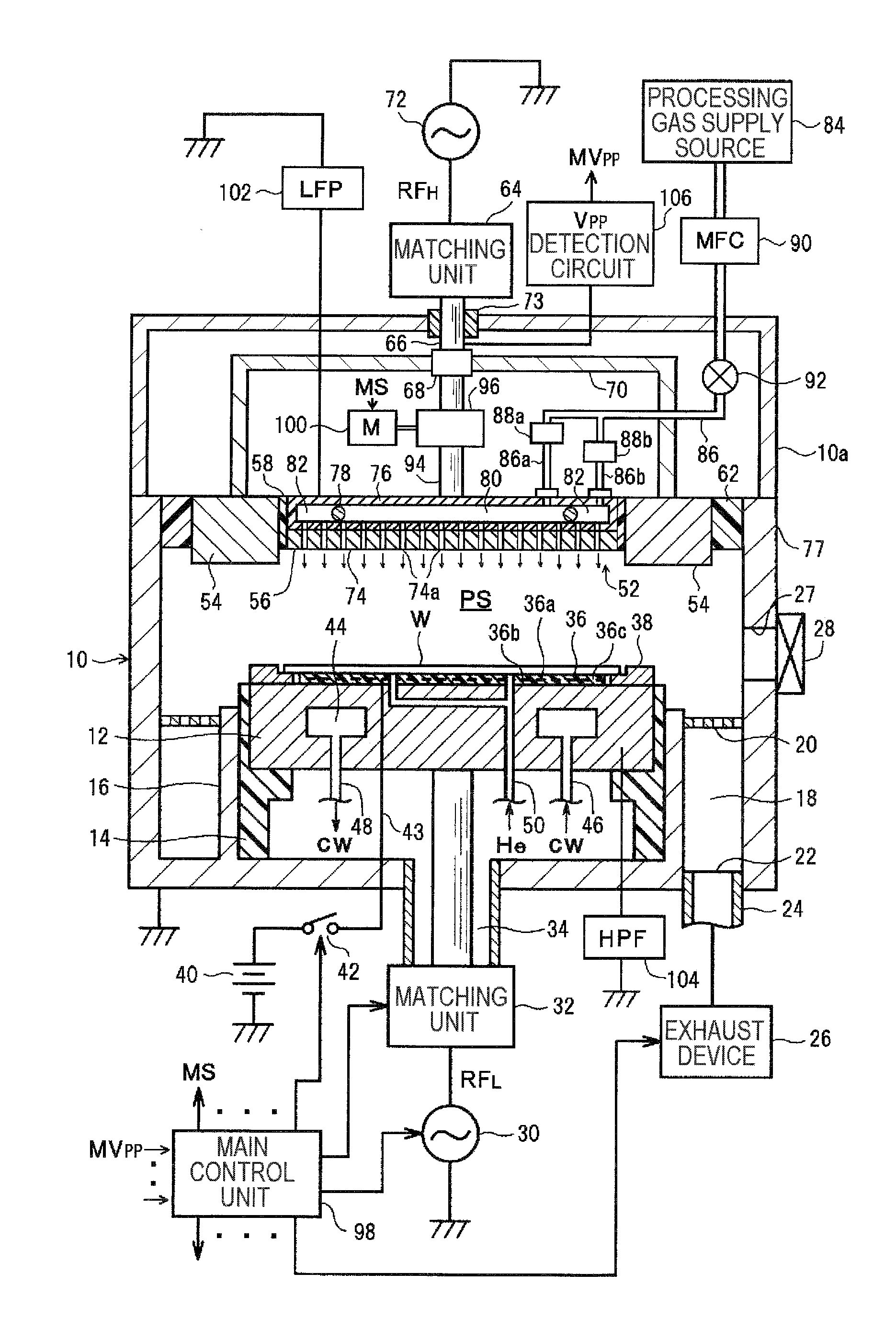
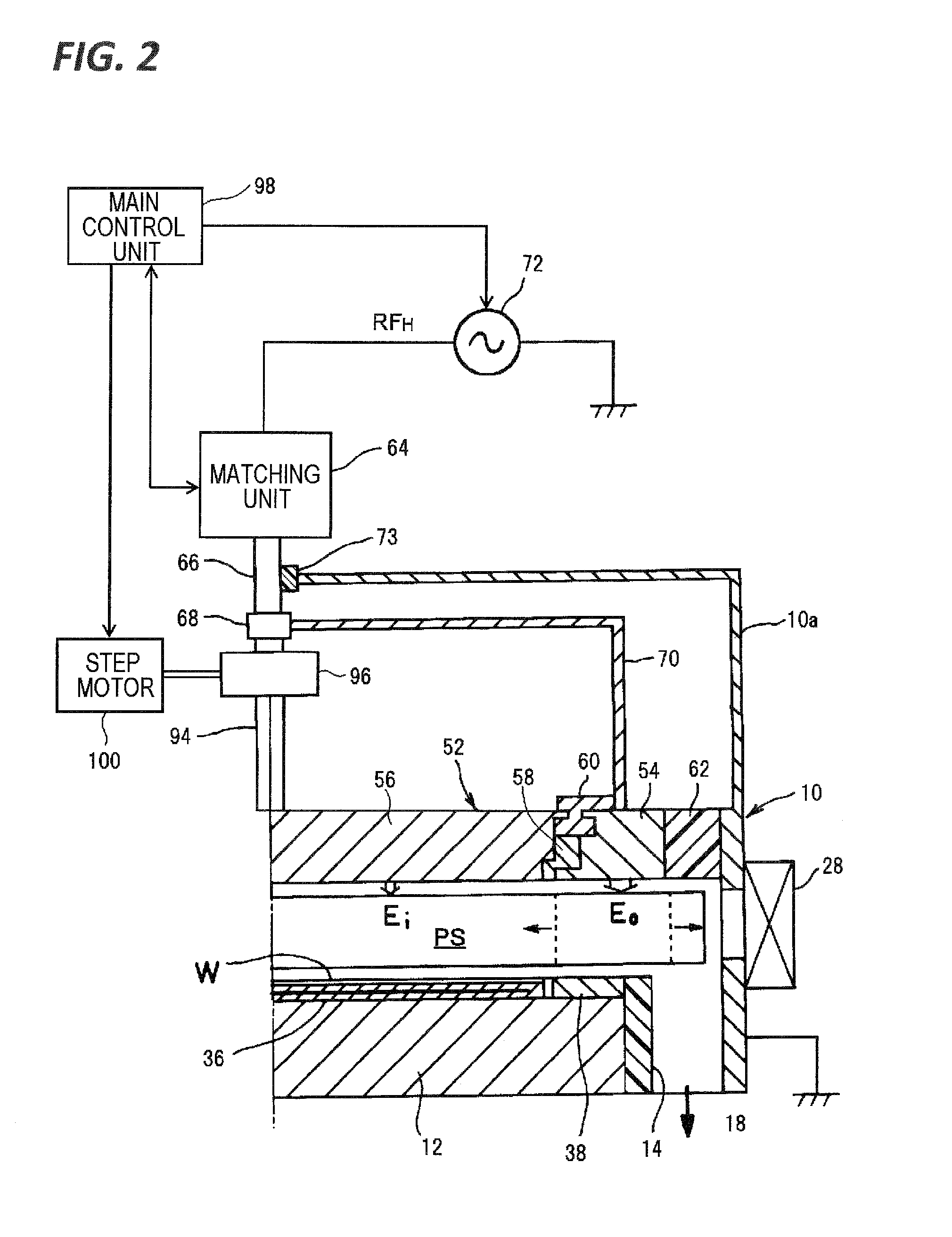
[0077]In the plasma processing apparatus of the exemplary embodiment, the present inventors selected four kinds of variable condenser positionings of the variable condenser 96, that is, ‘36’, ‘93’, ‘110’, and ‘130’ and conducted an etching test of a photoresist film using an SiO2 film as a mask. In the etching of the photoresist film, as main process conditions, a mixed gas of O2 / Ar (flow rate 20 / 200 sccm) was used as an etching gas, the pressure in the chamber 10 was set to 10 mTorr, the output of the upper high-frequency power supply 72 was set to 500 W, and the output of the lower high-frequency power supply 30 was set to 300 W.

[0078]Meanwhile, there is a correlation between the variable condenser positioning CPI of the variable condenser 96 and the peak-to-peak value Vpp of the high-frequency waves RFH, as illustrated in FIG. 7. The main control unit 98 has data of the correlation in a table on a memory, and may monitor Vpp through a Vpp detection circuit 106 to perform interloc...

example 2

[0083]In the plasma processing apparatus of the exemplary embodiment, the present inventors selected three kinds of variable condenser positionings of the variable condenser 96, that is, ‘36’, ‘88’, and ‘110’ and conducted an etching test of a multilayer film including an antireflective film (Si) and an organic film (carbon). In a first etching step of the antireflective film (Si), a mixed gas of CF4 / CHF3 / O2 (flow rate 150 / 75 / 35 sccm) was used in a processing gas, the pressure in the chamber 10 was set to 10 mTorr, the output of the upper high-frequency power supply 72 was set to 500 W, and the output of the lower high-frequency power supply 30 was set to 50 W. In a second etching step of the organic film (carbon), a mixed gas of O2 / Ar (flow rate 20 / 200 sccm) was used as an etching gas, the pressure in the chamber 10 was set to 10 mTorr, the output of the upper high-frequency power supply 72 was set to 500 W, and the output of the lower high-frequency power supply 30 was set to 300 ...

example 3

[0089]In the plasma processing apparatus of the exemplary embodiment, the present inventors has conducted a test and found that a phenomenon (characteristic) of the plasma density distribution characteristic or the in-plane profile of the process characteristic varied depending on abrasion of the upper electrode 52 (54, 56) may be well corrected or cancelled by adjusting the variable condenser positioning of the variable condenser 96.

[0090]In the test, as Comparative Example, the variable condenser positioning CPI of the variable condenser 96 was fixed to ‘36’, and three thicknesses CEL of the electrode plate 74 of the inner upper electrode 56 were selected as ‘15 mm’, ‘10 mm’, and ‘3 mm’ to etch a photoresist. In addition, as Example, when the thicknesses CEL of the electrode plate 74 were selected as ‘15 mm’, ‘10 mm’, and ‘3 mm’, the variable condenser positionings CPI of the variable condenser 96 were selected as ‘36’, ‘120’, and ‘112’, respectively, and others were used under th...


PUM

PropertyMeasurementUnit
frequencyaaaaaaaaaa
frequencyaaaaaaaaaa
sizeaaaaaaaaaa

Abstract

The present disclosure provides a method of performing a plasma processing on a substrate by using a plasma processing apparatus including a processing container; an outer upper electrode provided to face a lower electrode; an inner upper electrode disposed inside the outer upper electrode; a first high-frequency power supply; a first power feeding unit; a second power feeding unit; and a variable condenser. The first and second power feeding units, a fixed condenser formed between the outer upper electrode and the inner upper electrode, and a closed circuit including the variable condenser become a resonance state when the variable condenser has a capacitance value in a predetermined resonance region. The method includes selectively using a capacitance value in a first region lower than the resonance region of the variable condenser and a capacitance value in a second region higher than the resonance region to perform the plasma processing.

Description

TECHNICAL FIELD[0001]The present disclosure relates to a capacitively coupled plasma processing apparatus that variably controls a ratio of high-frequency powers distributed and supplied to inner and outer upper electrodes disposed to face a lower electrode on which a substrate is placed.BACKGROUND[0002]For a micromachining or processing such as, for example, etching, deposition, oxidation, or sputtering in a manufacturing process of a semiconductor device or a flat panel display (FPD), plasma is used to subject processing gas to an excellent reaction at a relatively low temperature. Discharge is typically used for generating plasma. Plasma processing apparatuses are generally classified into a plasma processing apparatus using high-frequency discharge and a plasma processing apparatus using microwave discharge. High-frequency discharge systems are also classified into a capacitively coupled system in which a parallel flat panel electrode is provided within a processing container an...

Claims


Application Information

Patent Timeline
Patent Type & Authority Applications(United States)
IPC IPC(8): H01J37/32
CPCH01J37/32568H01J37/32541H01J37/3244H01J37/32091H01L21/3065H01L21/31116H01L21/31122H01L21/31138H01J37/32174H01J37/32449H05H2242/26
Inventor KIHARA, YOSHIHIDEKAWAMATA, MASAYAHAGA, TOSHIO
Owner TOKYO ELECTRON LTD
Why Eureka
Try Eureka