

Semiconductor device
a technology of semiconductor devices and semiconductors, applied in semiconductor devices, semiconductor/solid-state device details, electrical apparatus, etc., can solve problems such as latchup breakdown and damage to circuits and components, and achieve the effect of increasing the latchup breakdown resistance of semiconductor devices
- Summary
- Abstract
- Description
- Claims
- Application Information
AI Technical Summary
Benefits of technology
Problems solved by technology
Method used
Image

Examples
first preferred embodiment
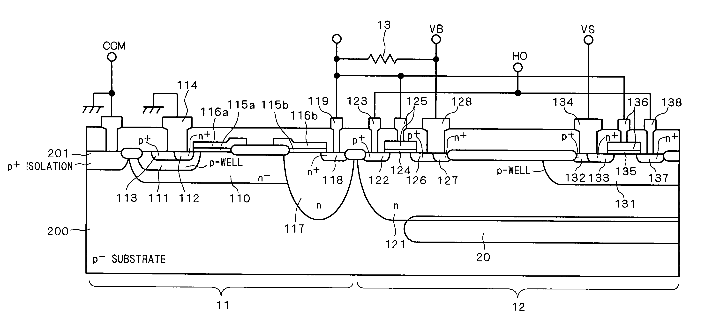
[0120]FIG. 1 is a cross-sectional view of the structure of the high-voltage-side driving section 101 according to a first preferred embodiment of this invention, taken along the line B-B in FIG. 57. As shown, in the upper surface of the p− substrate 200, a p+ isolation 201, the n−-type impurity region 110, and the n-type impurity regions 117 and 121 are formed. In the upper surface of the n-type impurity region 121, the p-well 131 is formed. The p+ isolation 201 reaches the p− substrate 200 having the lowest potential (GND potential or COM potential) in circuit. The p-well 111 is formed under the n+-type source region 112 of the high breakdown voltage MOS 11 to reach the bottom of the gate electrode 116a via a gate insulating film 115a, to form a channel region of the high breakdown voltage MOS 11. In the upper surface of the p-well 111, a p+-type impurity region 113 and the n+-type source region 112 are formed in contact with the source electrode 114. In the upper surface of the n-...
second preferred embodiment
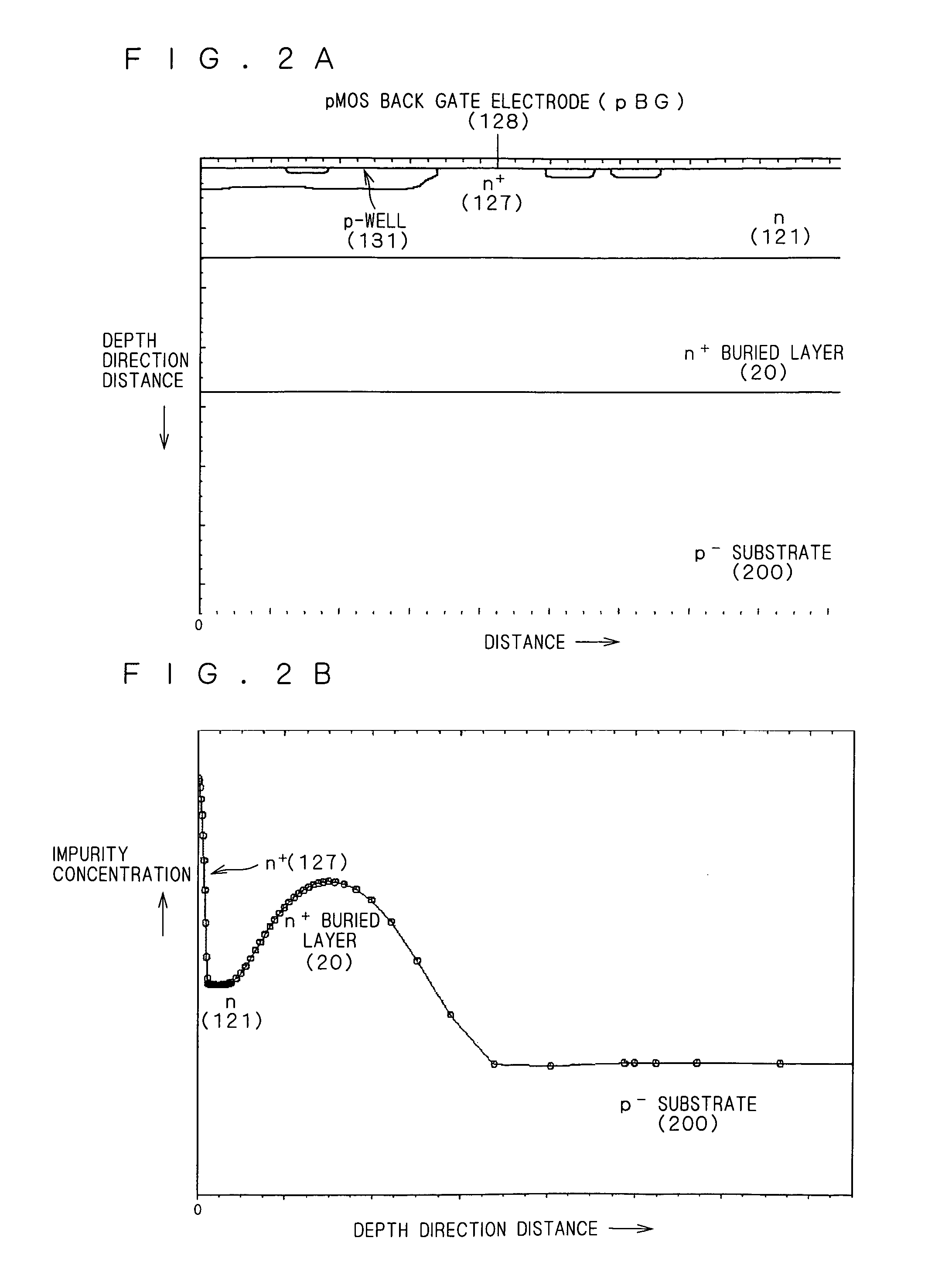
[0134]FIG. 8 is a cross-sectional view of the structure of the high-voltage-side driving section 101 according to a second preferred embodiment of this invention, correspondingly to FIG. 1. Instead of the n+ buried layer 20 in FIG. 1, an n+-type impurity region (hereafter called “n+ buried layer”) 22 having an impurity concentration higher than that of the n+ buried layer 20 is formed. By way of example, the peak value of impurity concentration of the n+ buried layer 22 is of the order of 1018 cm−3. As with the n+ buried layer 20, the n+ buried layer 22 is formed in contact with the bottom surface of the n-type impurity region 121 in the p− substrate 200.
[0135]FIG. 9A shows a simplified structure of the CMOS part according to the second preferred embodiment, correspondingly to FIG. 2A. FIG. 9B shows an impurity concentration profile from the upper surface of the n+-type impurity region 127 toward the depth direction of the p− substrate 200 with respect to a position where the pMOS b...
third preferred embodiment
[0141]FIG. 13 is a cross-sectional view of the structure of the high-voltage-side driving section 101 according to a third preferred embodiment of this invention, correspondingly to FIG. 1. Instead of the n+ buried layer20 in FIG. 1, an n+-type impurity region (hereafter called “n+ buried layer”) 23 having an impurity concentration higher than that of the n-type impurity region 121, and an n-type impurity region (hereafter called “n-buried layer”) 24 having an impurity concentration lower than that of the n+ buried layer 23 are formed. By way of example, the peak value of impurity concentration of the n+ buried layer 23 is of the order of 1018 cm−3, and the peak value of impurity concentration of the n-buried layer 24 is of the order of 1015 cm−3. As with the n+ buried layer 20, the n+ buried layer 23 is formed in contact with the bottom surface of the n-type impurity region 121 in the p− substrate 200. The n-buried layer 24 is formed to cover the circumference of the n+ buried laye...
PUM
 Abstract
Description
Claims
Application Information