Dual port SRAM with dedicated read and write ports for high speed read operation and low leakage

a read and write operation and dual-port technology, applied in the field of memory devices, can solve the problems of reducing the functionality of the dual-port sram cell, affecting the performance of the memory device, and defeating the very purpose of the dual-port sram, i.e., the ability to perform simultaneously read and write operations, etc., to achieve low static leakage, high-speed read operations, and easy cell fabrication

Inactive Publication Date: 2010-10-12
STMICROELECTRONICS PVT LTD
View PDF5 Cites 25 Cited by
  • Summary
  • Abstract
  • Description
  • Claims
  • Application Information

AI Technical Summary

Benefits of technology

[0015]According to the present invention a dual port static random access memory (SRAM) for high speed read operations is provided. The circuit and method of the present invention provides a dual port SRAM having low static leakages. The circuit and method of the present invention further provides a dual port SRAM utilizing a minimal cell area for easy cell fabrication.
[0016]The present invention provides a dual port SRAM having dedicated read and write ports to provide a high speed read operation with a low leakage. The SRAM of the present invention includes:
[0026]the at least one inverter circuit and pull down circuit being operatively coupled to the at least one cell to increase read operation performance and minimize leakage.
[0027]Further the present invention provides a method of providing a high speed read operation and a low leakage in a dual port SRAM including the steps of:

Problems solved by technology

The necessity of supporting information processing needs have made memory devices and systems more and more complex and diversified.
This results in crosstalk and brings about a characteristic drop in the dual port SRAM cell.
However, this defeats the very purpose of dual port SRAM, i.e., the ability to perform simultaneously the read and write operations.
This results in further degradation of speed as pass gates and latch NMOS transistors come in series both with high Vt implant.
However, this method presents another problem, in that the read enable RE has to drive all the bit lines and that requires a very wide metal line for RE (to eliminate risk of electro migration) as illustrated in FIG. 3.
As the size of the metal line is very wide, the metal line will not fit into a memory cell's height.
Also, due to huge current flowing in RE line, there is a rise in the voltage level of this signal which severely impacts performance of the last column (as the rise will be the maximum in the last column).
In addition, the size of a pull down NMOS driving the RE to ground needs to be very big, which causes a big static power loss (as this pull down will have Vds=Vdd available).
Also, it suffers from dynamic leakage on bit lines.
A larger size of the pass gate, will result in larger dynamic leakage.
However, as large numbers of gates are used in the memory cell itself, a large area is required, and dynamic as well as the static leakage of this cell will be even greater than the previous methods.
However, this will degrade the cell's performance drastically.
To improve read performance in the above configuration, only the read pass gates and corresponding pull downs are kept in logic thresholds, unfortunately at the expense of leakage.
However, this structure suffers from risks arising due to mixing of logic and SRAM (relatively high threshold voltage devices) and requires a big area increase to follow normal Design Rules Checking (DRC) to separate logic and SRAM devices.
Moreover, there is a reliability risk of repeated mixing of logic (low Vt) implant and SRAM (high Vt) implant.
The prior art discussed above does not overcome the major prevailing problems in the field of dual port SRAM for simultaneous read and write operations.
Problems like lower speed due to interactions between read and write ports, a very wide metal line for read enable (RE) signal, static power loss due to big pull down transistor for RE, dynamic and static leakages, asymmetric structure and bigger area, etc., still persists.

Method used


Image

  • Dual port SRAM with dedicated read and write ports for high speed read operation and low leakage
  • Dual port SRAM with dedicated read and write ports for high speed read operation and low leakage
  • Dual port SRAM with dedicated read and write ports for high speed read operation and low leakage

Examples


Embodiment Construction

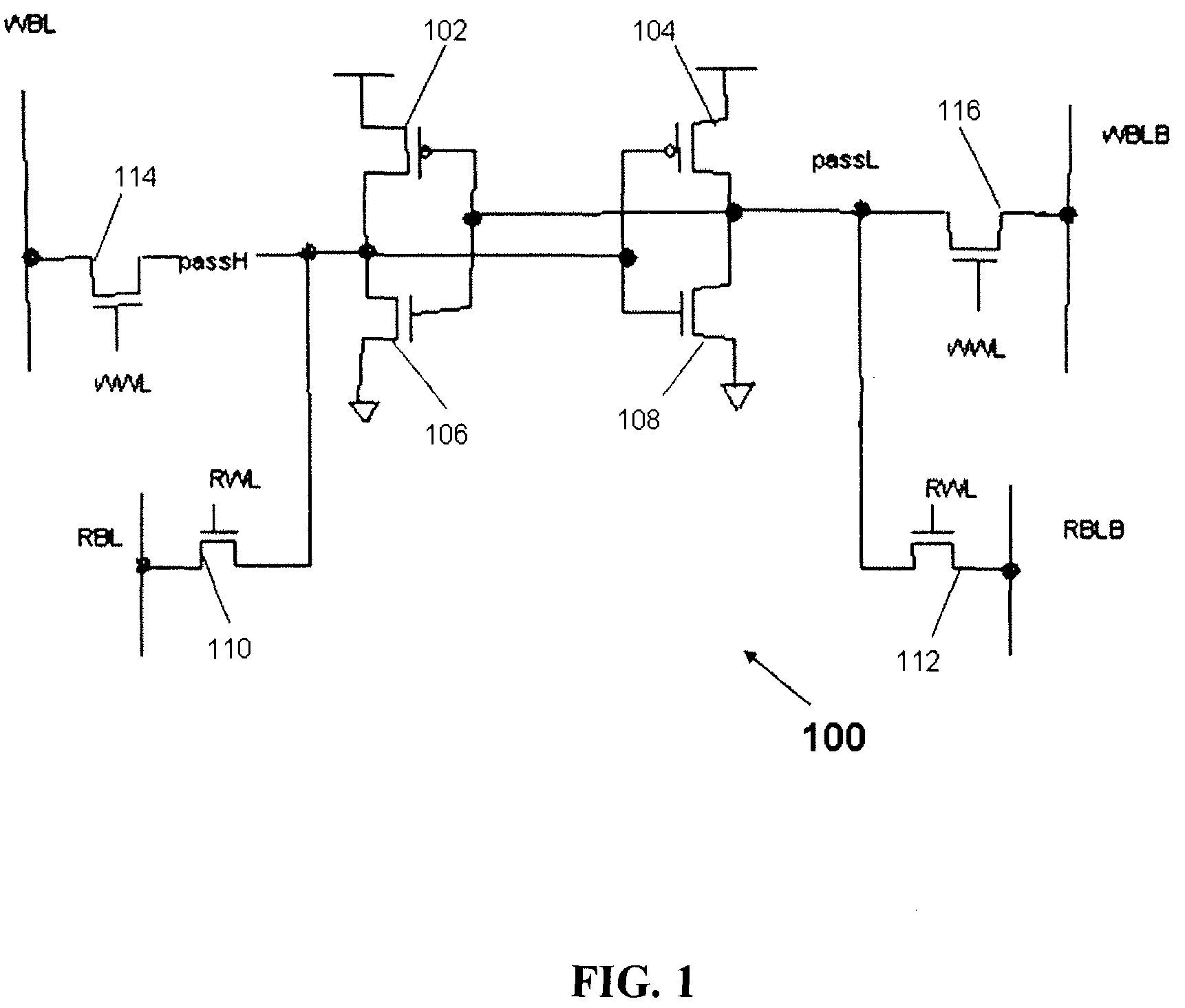
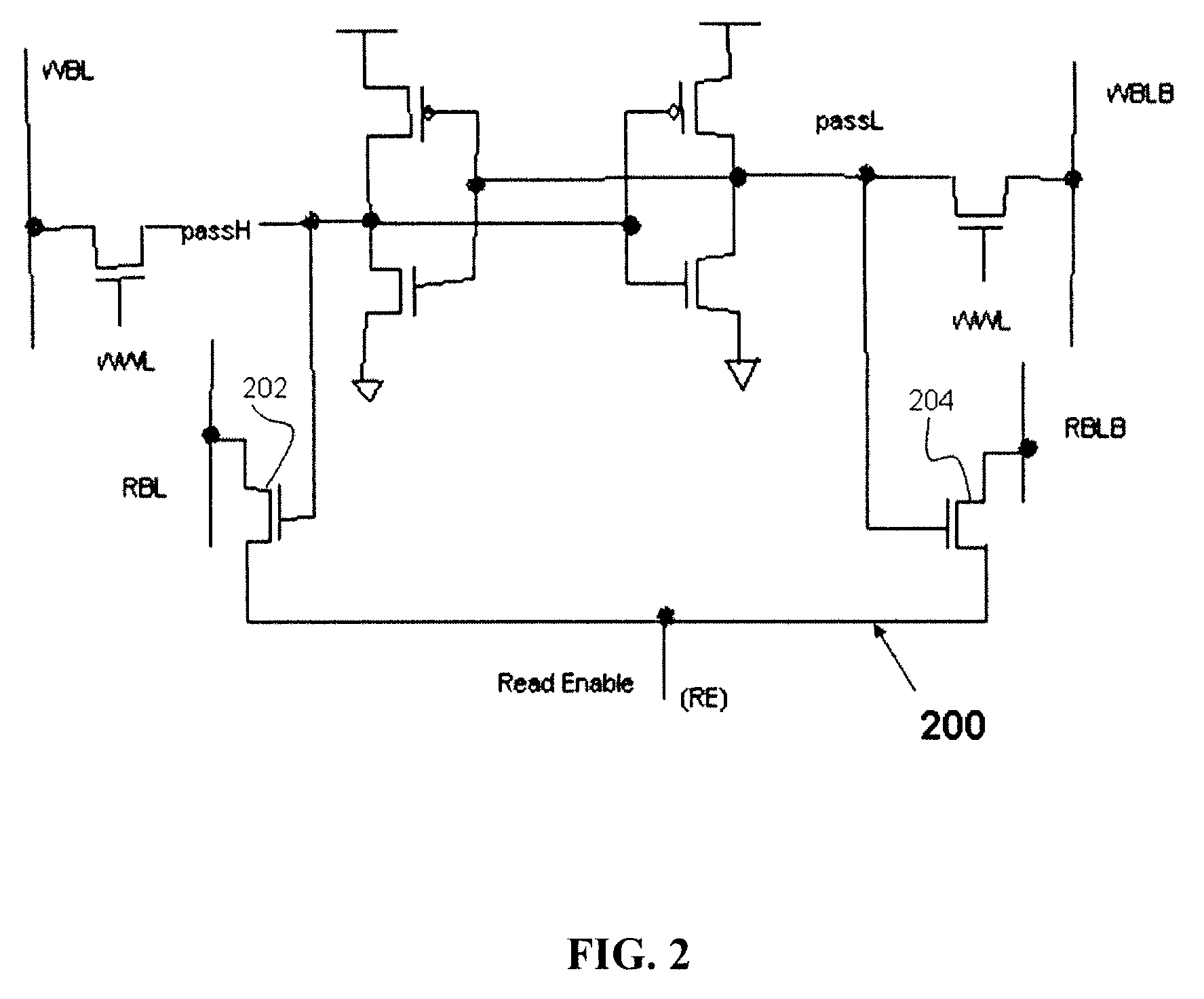
[0038]The preferred embodiments of the present invention will be described in detail with reference to the accompanying drawings. However, the present invention is not limited to the preferred embodiments. The present invention can be modified in various forms. The preferred embodiments of the present invention are only provided to explain more clearly the present invention to the ordinarily skilled in the art of the present invention. In the accompanying drawings, like reference numerals are used to indicate like components.

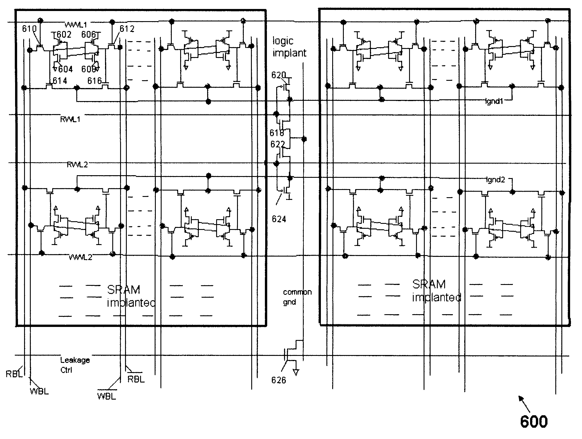
[0039]The present invention provides a SRAM architecture for high speed read operation with a dedicated read and write port with a minimal area. In the present invention, the dual port SRAM has an organized cell positioned in a plurality of rows and columns.

[0040]FIG. 6 illustrates an architecture for an SRAM array 600 according to the present invention. Dual port static random access memories (SRAM) having dedicated read and write ports. The SRAM array provides...


PUM


Abstract

A dual port static random access memory (SRAM) having dedicated read and write ports provides high speed read operation with reduced leakages. The dual port SRAM includes at least one write word line, at least one read word line, at least one pair of write bit line and read bit line, a plurality of rows and columns. Each rows and column has at least one cell which includes at least one pair of memory elements cross-coupled to form a latch for storing data, a pair of write access semiconductors and a pair of read access semiconductors. The SRAM includes an inverter circuit and a pull down circuit which are operatively coupled to the at least one cell to increase read operation performance and eliminate leakage.

Description

RELATED APPLICATION[0001]The present application claims priority of Indian Patent Application No. 1947 / Del / 2006 entitled DUAL PORT SRAM WITH DEDICATED READ AND WRITE PORTS FOR A HIGH SPEED READ OPERATION AND A LOW LEAKAGE, and filed Aug. 30, 2006, which is incorporated herein in its entirety by this reference.FIELD OF THE INVENTION[0002]The present invention relates to memory devices, and more specifically to a dual port static random access memory (SRAM) architecture providing a high speed read operation with reduced leakage.BACKGROUND OF THE INVENTION[0003]The necessity of supporting information processing needs have made memory devices and systems more and more complex and diversified. Moreover, it has become highly advantageous to execute read and write operations simultaneously. This has led to the advent of dual port memory, which provides two access ports (e.g., left and right ports) that can access a common memory array. Dual port memory allows one port to be used for a writ...

Claims


Application Information

Patent Timeline
Patent Type & Authority Patents(United States)
IPC IPC(8): G11C13/00
CPCG11C8/16
Inventor LUTHRA, YOGESH
Owner STMICROELECTRONICS PVT LTD
Why Eureka
Try Eureka