Thin film solar cell manufacturing and integration

a technology of thin film solar cells and solar cells, applied in the manufacture of final products, manufacturing tools, coatings, etc., can solve the problems of reducing the yield deteriorating the efficiency of modules manufactured using thin film solar cells, and higher electricity generation cost of silicon-based solar cells than the cost of electricity generated by the more traditional methods

Inactive Publication Date: 2010-11-02
SOLOPOWER
View PDF10 Cites 64 Cited by
  • Summary
  • Abstract
  • Description
  • Claims
  • Application Information

AI Technical Summary

Problems solved by technology

However, the cost of electricity generated using silicon-based solar cells is higher than the cost of electricity generated by the more traditional methods.
Such shorts reduce yield and deteriorate efficiency of the modules manufactured using thin film solar cells.

Method used


Image

  • Thin film solar cell manufacturing and integration
  • Thin film solar cell manufacturing and integration
  • Thin film solar cell manufacturing and integration

Examples


Embodiment Construction

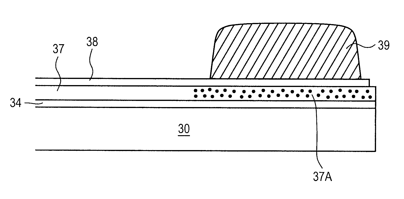
[0028]The present invention provides a method for forming a solar cell absorber layer with an active portion and an electrically resistive portion. The electrically resistive portion or resistive portion increases resistance between an underlying base layer and a connector layer. A transparent conductive layer is between the absorber layer and the connector layer. The connector layer or the finger patterns comprises the busbar and the fingers of the solar cell. The busbar is preferably placed over the electrically resistive portion while the fingers extend over the active portion of the absorber layer. The absorber layer may be a Group IBIIIAVIA compound layer and may be formed by first forming a precursor stack including Group IB, Group IIIA and Group VIA materials. The precursor stack may be formed by sequentially depositing the layers of Group IB, Group IIIA and Group VIIA materials.

[0029]In one embodiment, the resistive portion may be formed by masking a portion of the base whil...


PUM

PropertyMeasurementUnit
molar ratioaaaaaaaaaa
thicknessesaaaaaaaaaa

Abstract

A method of forming a Group IBIIIAVIA solar cell absorber which includes an active portion and an electrically resistive portion. The absorber is interposed between a base layer and a transparent conductive layer. The electrically resistive portion increases resistance between the base layer and a connector layer that is formed on the transparent conductive layer. The connector layer comprises the busbar and the fingers of the solar cell. The busbar is preferably placed over the electrically resistive portion while the fingers extend over the active portion of the absorber layer.

Description

CROSS-REFERENCE TO RELATED APPLICATIONS[0001]This application claims the benefit of provisional application Ser. No. 60 / 883,336 filed on Jan. 3, 2007.BACKGROUND[0002]1. Field[0003]The present invention relates to thin film solar cell structures and methods of manufacturing them.[0004]2. Description of the Related Art[0005]Solar cells are photovoltaic (PV) devices that convert sunlight directly into electrical power. The most common solar cell material is silicon, which is in the form of single or polycrystalline wafers. However, the cost of electricity generated using silicon-based solar cells is higher than the cost of electricity generated by the more traditional methods. Therefore, since early 1970's there has been an effort to reduce cost of solar cells for terrestrial use. One way of reducing the cost of solar cells is to develop low-cost thin film growth techniques that can deposit solar-cell-quality absorber materials on large area substrates and to fabricate these devices us...

Claims


Application Information

Patent Timeline
Patent Type & Authority Patents(United States)
IPC IPC(8): H01L31/0224H01L31/0256
CPCH01L31/03928H01L31/06H01L31/0749H01L31/1884H01L31/0504H01L31/046H01L31/0201H01L31/0322Y02E10/541Y02P70/50
Inventor BASOL, BULENT M.
Owner SOLOPOWER
Why Eureka
Try Eureka