Direct dipping cooled power module and packaging

a technology of power modules and power modules, applied in the field of power modules, can solve the problems of high operating temperature, serious affecting the lifetime and/or reliability of power modules, and the inherent temperature limitations of semiconductor devices and associated packaging materials, so as to reduce parasitic inductance and improve electrical performan

Inactive Publication Date: 2009-09-17
FORD GLOBAL TECH LLC
View PDF28 Cites 47 Cited by
  • Summary
  • Abstract
  • Description
  • Claims
  • Application Information

AI Technical Summary

Benefits of technology

[0019]According to another aspect of the invention, a power module package is provided with improved electrical performance including, folded circuitry layout to cancel the parasitic effects, as well as the compact power terminals, to reduce the parasitic inductance inside and outside from module to power busbar.

Problems solved by technology

During operation, the die dissipate large amounts of heat, on the order of hundreds watts (W) per die, leading to high operating temperatures.
Semiconductor devices and associated packaging materials present inherent temperature limitations.
For example, the maximum operating temperature of a silicon (Si) device is about 150° C. Furthermore, high temperature and large temperature excursion during their operation seriously affect the lifetime and / or reliability of power modules.
For example, due to complex cooling configuration, such prior art modules have serious limitations including undesirably high thermal resistance, poor thermo-mechanical reliability, undesirably high weight, and undesirably high cost of manufacture, as well as producing undesired electrical parasitic effects caused by lack of special electrical considerations.

Method used


Image

  • Direct dipping cooled power module and packaging
  • Direct dipping cooled power module and packaging
  • Direct dipping cooled power module and packaging

Examples


Embodiment Construction

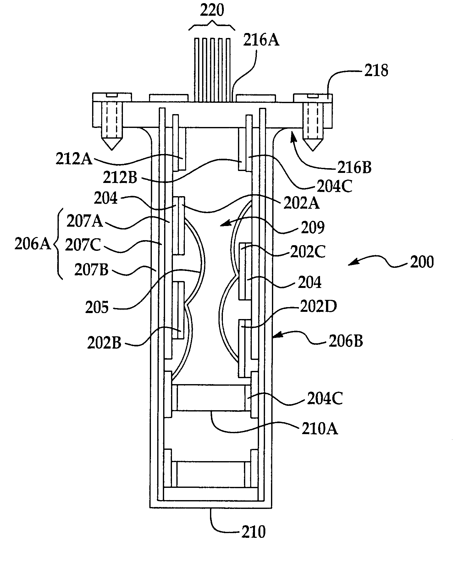
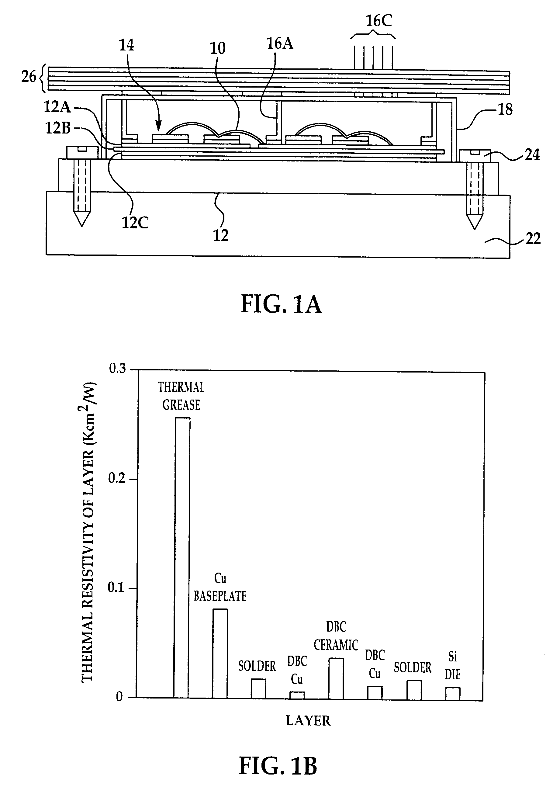
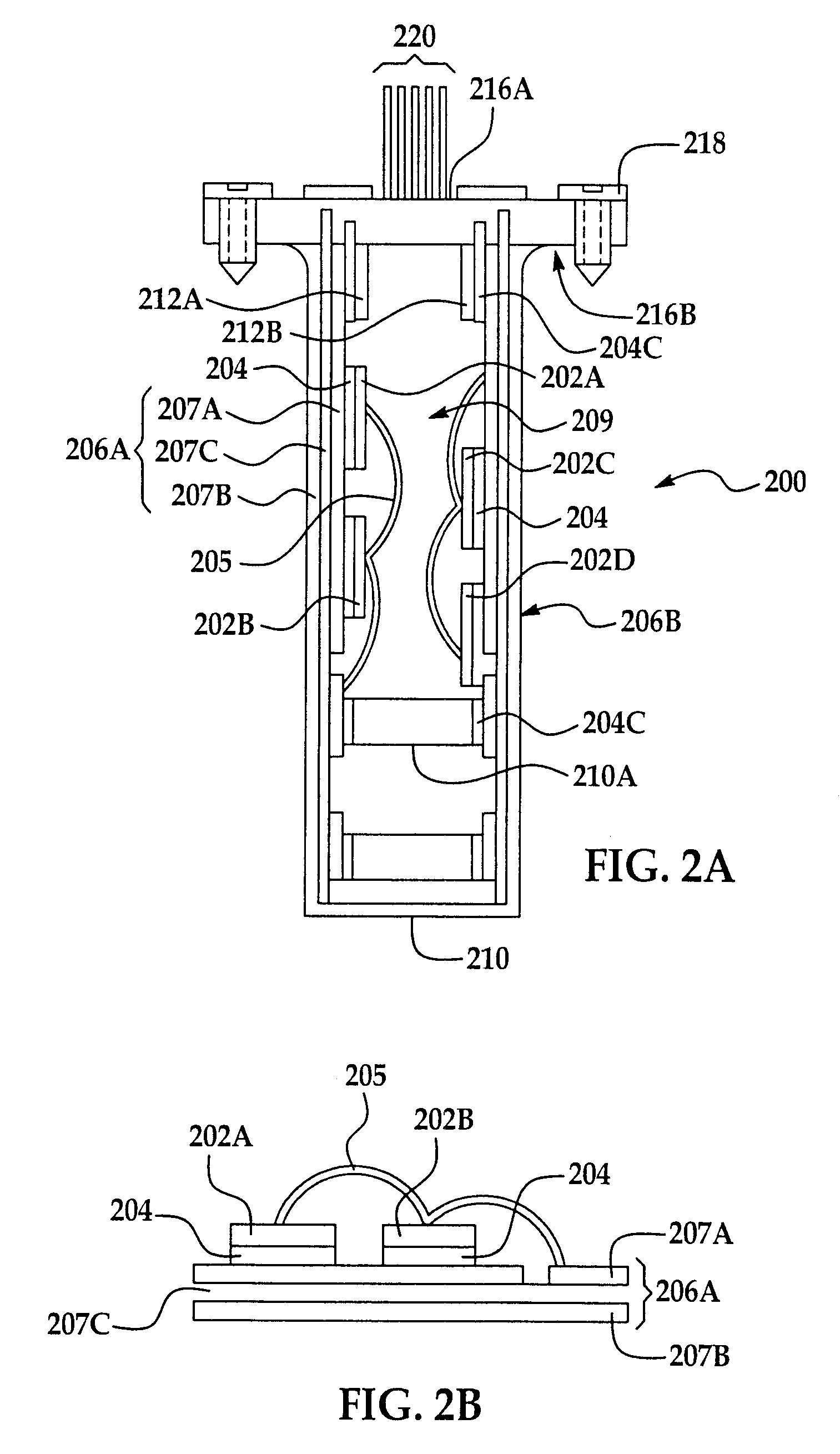
[0033]The present invention achieves the foregoing objects, aspects and features by providing circuit elements, such as semiconductor die forming a portion of a power module package, mounted by direct bonding through a conductive layer to a conductive circuit substrate forming at least one sidewall of a fully enclosed power module package. The power module package includes at least one conductive circuit substrate with mounted circuit elements forming at least one sidewall of an enclosed and sealed power module package (container) where two sidewalls of the power module package have a greater width compared to two other sidewalls of the power module container to form a fin shaped structure, for example having a width greater by a factor of greater than 2, preferably greater than 3, even more preferably greater than 4.

[0034]The circuit elements directly bonded on the conductive circuit substrate forming a rectangular shaped sidewall of the power module package face inward to an enclo...


PUM


Abstract

A power module package including a fully enclosed package comprising sidewalls; wherein at least one of said sidewalls includes a conductive substrate; wherein circuit elements are mounted on said conductive substrate on a first side comprising an inner side of said enclosed package; and, wherein a majority area of a second side of said conductive substrate is exposed, the power package has an improved interconnection configuration and compact power I / O terminals, offering low electrical parasitics, a plurality of individual power module packages can be attached seamlessly and positioned in a liquid coolant with multiple top portion open channels, as well as attached to a laminar power connector (busbar) to form various electrical power conversion topologies, the module offers low thermal resistance and low electrical parasitics, in addition to small volume, light weight and high reliability.

Description

FIELD OF THE INVENTION[0001]This invention generally relates to power modules including power semiconductor devices such as insulated gate bipolar transistors (IGBTs), power metal oxide semiconductor field effect transistors (MOSFETs), and diodes which function as electric power switching devices, and more particularly provides a novel power module package and power module package assembly to provide enhanced cooling and power dissipation while avoiding parasitic effects.BACKGROUND OF THE INVENTION[0002]Power semiconductor devices IGBTs, MOSFETs and diodes play the role of switching electric power at speeds of hundreds of kHz in power electronic conversion systems such as motor drives. The core element of these power switches is one or more semiconductor die (note the term die is used in both the singular and plural sense) each with a dimension of, for example 10 mm×10 mm×0.1 mm with rated current / voltage at hundreds of amperes (A) and hundreds of volts (V).[0003]To facilitate high ...

Claims


Application Information

Patent Timeline
Patent Type & Authority Applications(United States)
IPC IPC(8): H05K7/20H01L21/52
CPCH01L23/3735H01L23/473H01L25/071H01L2924/13091H01L2924/1305H01L2924/30107H01L2224/73265H01L2224/48472H01L2224/48091H01L2924/13055H01L2224/32225H01L2224/48137H01L2224/48227H01L2924/00H01L2924/00014H01L2224/48139H01L2224/49111H01L2924/00012
Inventor LIANG, ZHENXIANCHEN, CHINGCHIDEGNER, MICHAEL W.
Owner FORD GLOBAL TECH LLC
Why Eureka
Try Eureka