CA resistance variability prediction methodology

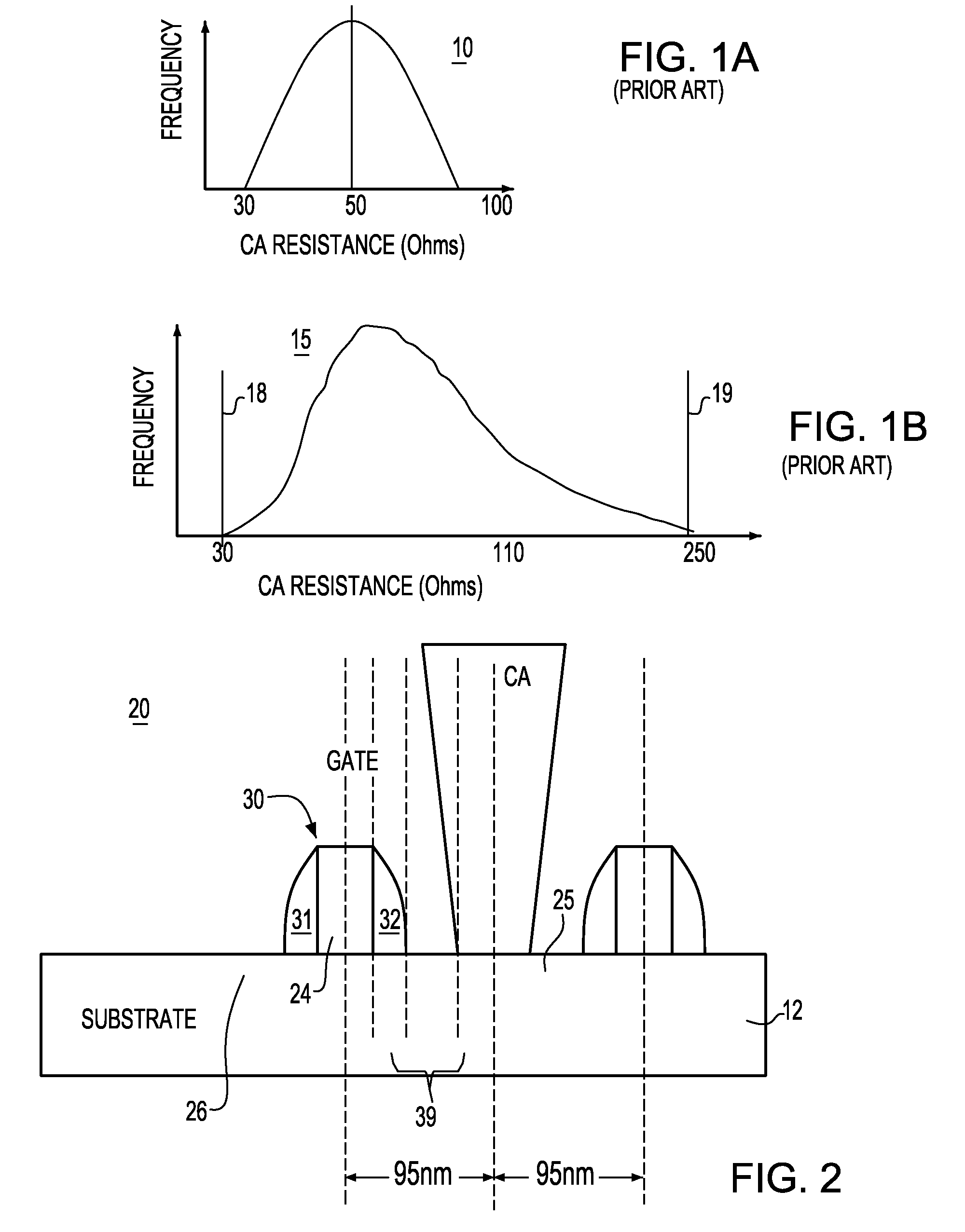
a resistance variability and prediction method technology, applied in the field of semiconductor circuit design and circuit performance modeling, can solve the problems of increasing variability with ever shrinking, affecting the accuracy of circuit design, and difficult to estimate the endpoints of the curve b>18/b> and b>19/b>, especially the upper curve endpoint b>19/b>

Active Publication Date: 2010-11-09
SIEMENS PROD LIFECYCLE MANAGEMENT SOFTWARE INC
View PDF7 Cites 5 Cited by
  • Summary
  • Abstract
  • Description
  • Claims
  • Application Information

AI Technical Summary

Benefits of technology

[0015]In one embodiment, a whole set of software tools to develop this algorithm, which includes a novel bucketization scheme, is implemented. This provides the circuit designer with considerably better design options for handling large CA variability as seen through the design manual.
[0024]utilizing the device parasitic netlist values to provide for more accurate circuit behavior modeling of circuits having the CA.

Problems solved by technology

Variability is a serious issue for circuit designers given that performance based Circuit Limiting Yield (CLY) is now a major concern.
The problem is that variability is rapidly increasing with ever shrinking technology nodes.
However, estimating the endpoints of the curve 18 and 19, particularly upper curve endpoint 19, is not always easy.
However, in 45 nm CMOS technology designs, there is limited room to increase CA size.
It is thus the case that CA size determines device performance and, it is the case that in some current designs, due to CA resistance variability, manufacturers are presented with major trade-off design issue between CA opens which tend to occur at the small CD, and PC-CA shorts which tend to occur at larger CD.
Thus, while the 65 nm CMOS technology need for yield is pushing the CA size to 100 nm which is currently achievable in 65 nm ground-rules, there is not enough room for this large a CA size in 45 nm CMOS technology.
On the other hand due to material issues associated with filling a small high-aspect ratio (CA) contact hole it is difficult to fill too small a CA.
That is, the calculated resistance from simple area calculations (RSS of SW taper, CA height, bottom CD, and resistivity) as modeled in prior art are inadequate.
Given the expected difficulty of creating yieldable CA structures, the issue of modeling CA variability is absolutely critical for CMOS circuit designers.

Method used


Image

  • CA resistance variability prediction methodology
  • CA resistance variability prediction methodology
  • CA resistance variability prediction methodology

Examples


Embodiment Construction

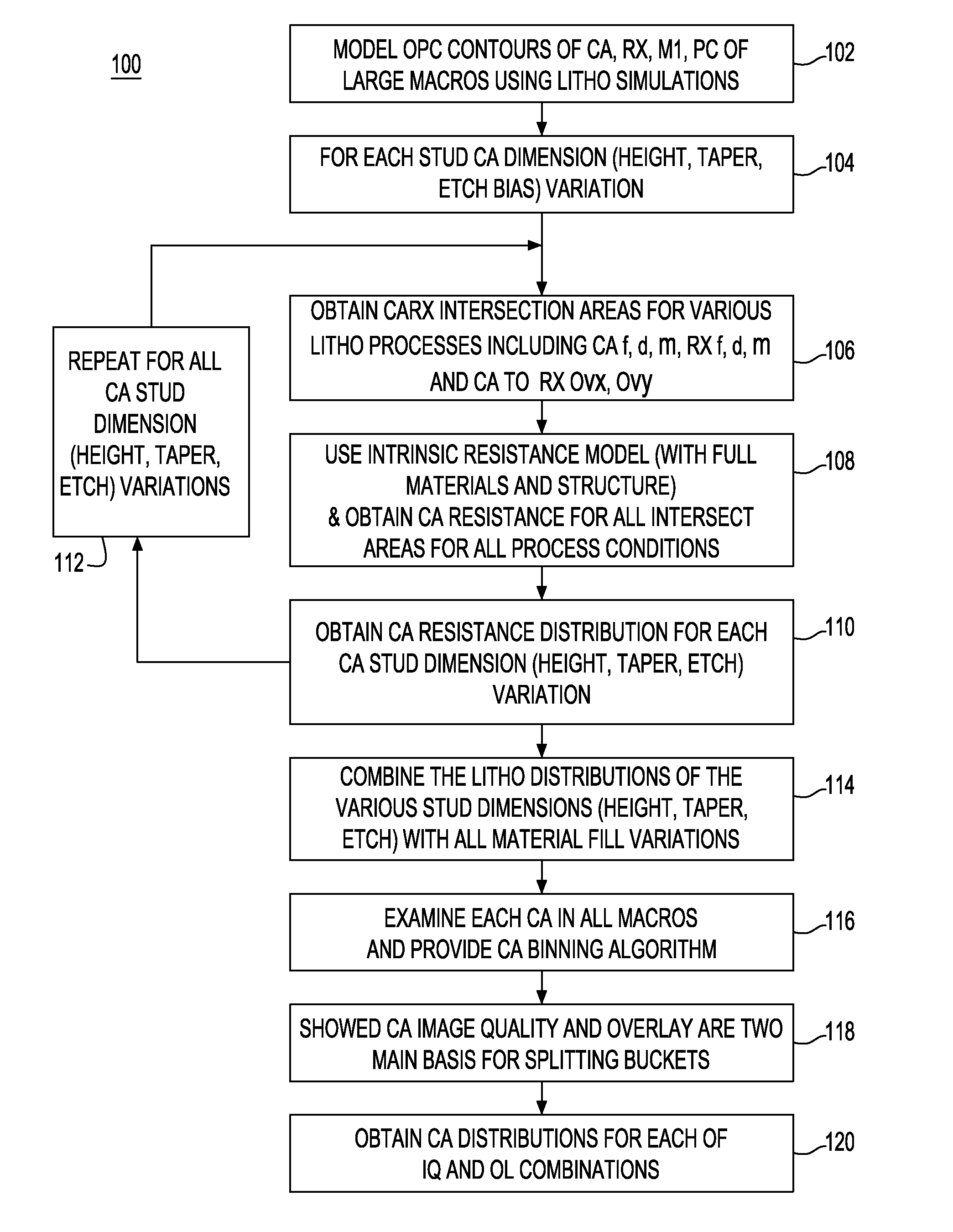
[0051]The present invention is directed to a methodology and algorithm to obtain a dramatically improved prediction of CA (Contact Via) resistance in electronic circuits; particularly, an improved CA resistance model adapted to capture larger than anticipated “out of spec” regime.

[0052]The novel algorithm and methodology implemented for improving CA resistance variability provides model results that can be codified and released through a Design Manual. In one aspect of the invention, a novel CA bucketization model is implemented, that, as will be described in greater detail herein, provide model results in the form of CA buckets and the respective resistance means / sigmas. In order to facilitate development of devices at the 45 nm and 32 nm technology level, these model results have to be added to the model / extraction suite and design kits and consequently, therefore have to facilitate extraction vendor tool developers (for tools such as Calibre, Assura, Hercules, etc.).

[0053]In one ...


PUM


Abstract

A methodology for obtaining improved prediction of CA resistance in electronic circuits and, particularly, an improved CA resistance model adapted to capture larger than anticipated “out of spec” regime. In one embodiment, a novel bucketization scheme is implemented that is codified to provide a circuit designer with considerably better design options for handling large CA variability as seen through the design manual. The tools developed for modeling the impact of CA variable resistance phenomena provide developers with a resistance model, such as conventionally known, modified with a new CA model Basis including a novel CA intrinsic resistance model, and, a novel CA layout bucketization model.

Description

BACKGROUND OF THE INVENTION[0001]1. Field of the Invention[0002]The present invention relates generally to semiconductor circuit design, and circuit performance modeling, and, more particularly, to a system and method for improving the prediction of contact resistance variability in semiconductor device contact structures.[0003]2. Description of the Prior Art[0004]Variability is a serious issue for circuit designers given that performance based Circuit Limiting Yield (CLY) is now a major concern. The problem is that variability is rapidly increasing with ever shrinking technology nodes.[0005]One major area of variability is the contact via (CA) resistance, a large component of which is layout proximity related. FIG. 1A shows the present CA Resistance Distribution Model used by circuit designers in 65 and 45 nm technologies. As shown in the plot 10 shown in FIG. 1A, based on input data comprising side-wall (SW) taper, CA height, and CA radius variations, it is seen that present CA va...

Claims


Application Information

Patent Timeline
Patent Type & Authority Patents(United States)
IPC IPC(8): G06F17/50
CPCG06F17/5036G06F30/367
Inventor CHIDAMBARRAO, DURESETIHENG, FOOK-LUENLAVIN, MARK A.LEE, JIN-FUWSINGH, RAMA N.TSAI, ROGER Y.
Owner SIEMENS PROD LIFECYCLE MANAGEMENT SOFTWARE INC
Why Eureka
Try Eureka