SCR controlled by the power bias

a power bias and power bias technology, applied in the field of circuit protection, can solve the problems of nodes that connect to power supplies, excessive current, and more of a problem of catching up

Active Publication Date: 2010-11-16
SEMICON COMPONENTS IND LLC
View PDF12 Cites 53 Cited by
  • Summary
  • Abstract
  • Description
  • Claims
  • Application Information

AI Technical Summary

Problems solved by technology

Damage to devices typically can be described as a catastrophic voltage breakdown of an oxide layer that destroys the device or as latch up where a device unexpectedly remains turned on.
As the NMOS devices get smaller, latch up becomes more of an issue.
These transistors are biased off, but when stressed by over voltage, heat, radiation, etc. the PN junctions may become forward biased in a regenerative manner and draw excessive current.
Generally nodes that that connect to power supplies, e.g., Vcc, are more susceptible to latch up while I / O pins are more susceptible to ESD voltage breakdowns.

Method used


Image

  • SCR controlled by the power bias
  • SCR controlled by the power bias
  • SCR controlled by the power bias

Examples


Embodiment Construction

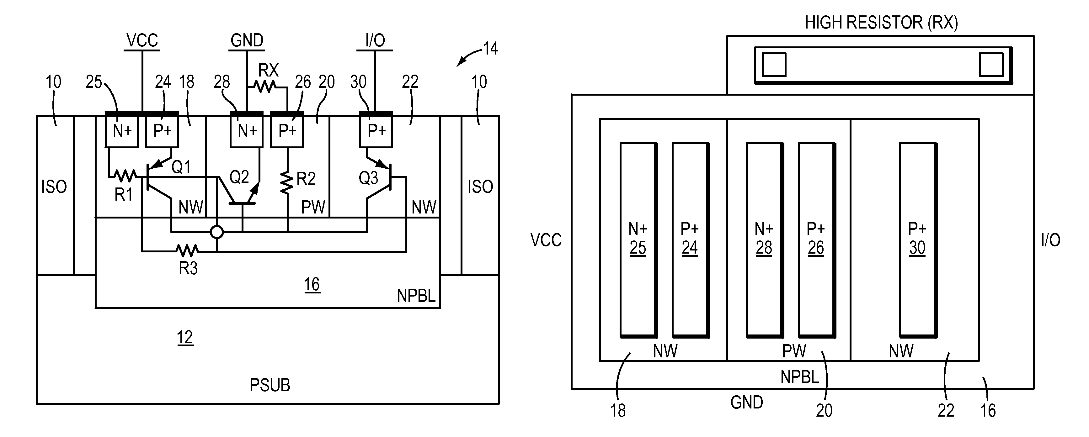
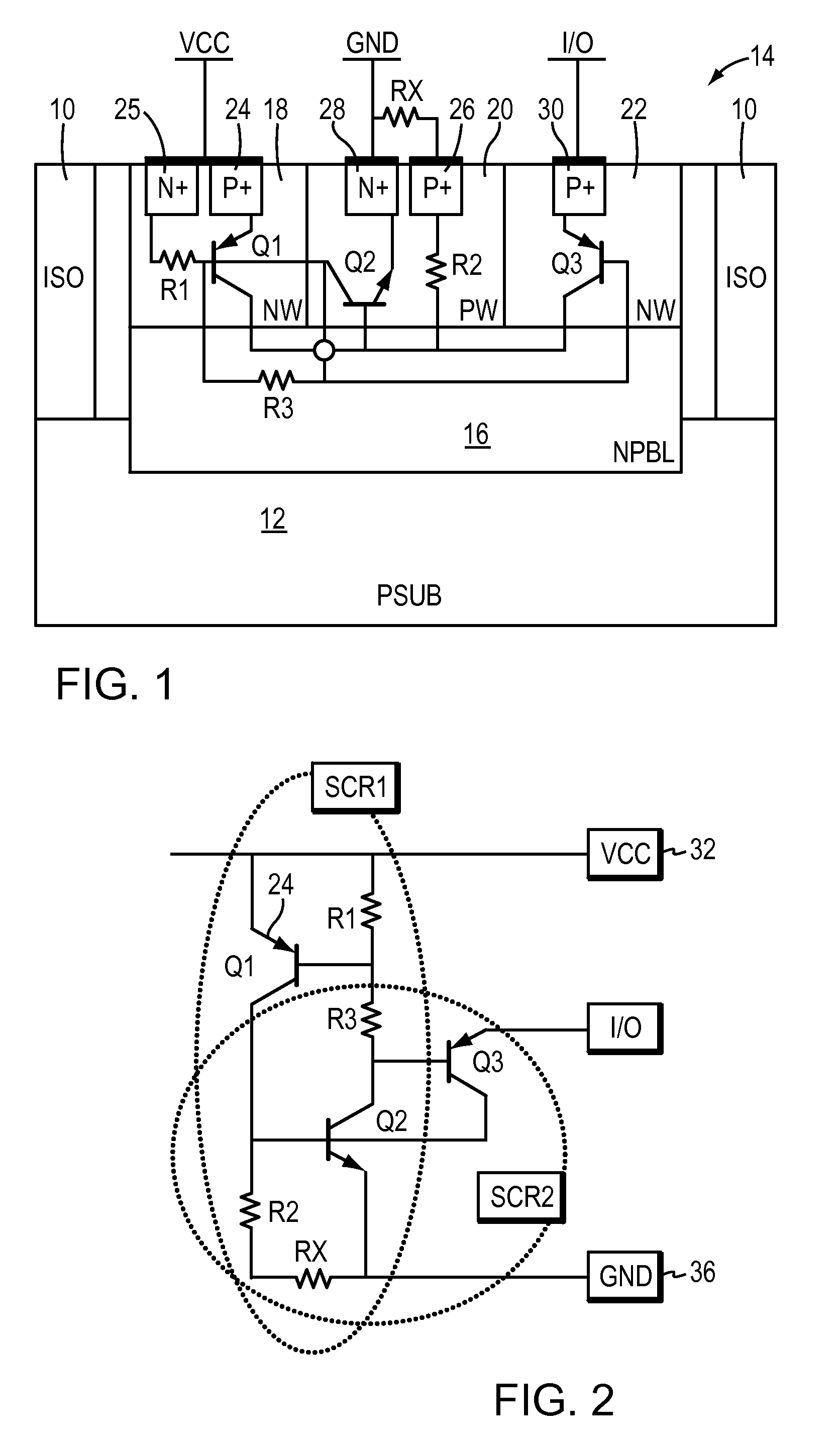
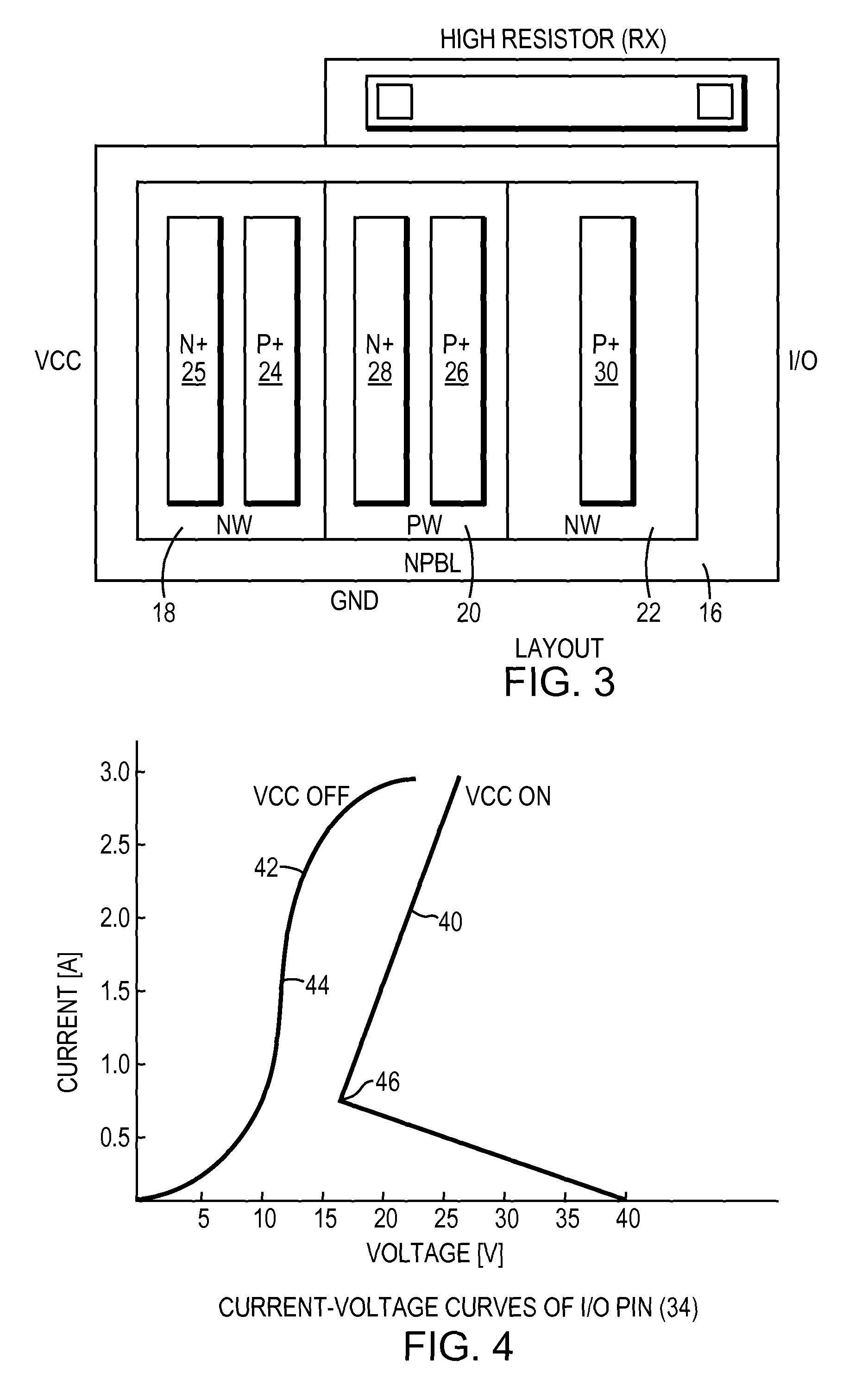
[0023]FIG. 1 shows an IC (integrated circuit) composite dual SCR and FIG. 2 is an equivalent circuit schematic. The dual SCR 14 shares a common circuit element, the NPN bipolar transistor Q2 of FIG. 2.

[0024]FIG. 1 shows isolation diffusions, ISOs 10, that connect to the P-type substrate 12 and isolate the dual SCR 14. An NPBL (N+-type buried layer) 16 underlies the dual SCR. Two NW 18 and 22 (N-type Wells) wells are formed on either side of a P+ well 20 that penetrates to the NPBL 16. A P+ electrode 24 is diffused in the NW 18 to form the emitter of PNP Q1. Q1 base is brought to an N+ electrode 25, and the base and the emitter of Q1 are connected together and tied to Vcc. An inherent resistor R1 exists in the base connection since the N-type structure 18 is not highly doped. The collector of Q1 connects via the NPBL 16 to the P+ electrode 26 in the P-type structure 20 through the resistance R2.

[0025]The base of Q1 also forms the collector of the NPN Q2, and the NPBL 16 forms the bas...


PUM


Abstract

A composite dual SCR circuit that acts to protect the Vcc node as well as an I / O node or pin. The dual SCR uses the Vcc to control or program the triggering point of the SCR connected to an I / O node. When Vcc is low, the SCR protecting an I / O node triggers a few volts above ground, but when Vcc is high the trigger point of the SCR protecting the I / O node is much higher. The dual SCR incorporates added diffusions to an existing first SCR structure between the power node and the ground node thereby forming a second SCR. The first and second SCRs share a common cathode transistor. In one illustrative embodiment, only one SCR is constructed incorporating the Vcc to control the triggering of the SCR.

Description

BACKGROUND OF THE INVENTION[0001]1. Field of the Invention[0002]The present invention relates to circuit protection from ESD (Electro Static Discharge, and more particularly to use of SCRs (Silicon Controlled Rectifiers) to protect against ESD events and latch up.[0003]2. Background Information[0004]Conventional ESD protection devices and methods include SCRs coupled across I / O (input / output) nodes that are directly coupled to the external environment and, thus, susceptible to external influences. Such SCRs are also connected across nodes that connect to power supplies. The protecting SCR, when positioned across two nodes (one node typically being ground), will present an open circuit to node voltages (meaning the voltage difference between the two nodes) less than the trigger or breakdown voltage of the SCR. When triggered by a voltage above the trigger voltage the SCR presents a low impedance across the pins as long as the node voltage is above the holding voltage of the SCR. Past...

Claims


Application Information

Patent Timeline
Patent Type & Authority Patents(United States)
IPC IPC(8): H01L29/74H01L23/62
CPCH01L27/0262H01L29/74H01L23/60H01L27/04
Inventor RYU, JUNHYEONGKANG, TAEGHYUNKIM, MOONHO
Owner SEMICON COMPONENTS IND LLC
Why Eureka
Try Eureka