Optical holographic device with a hologram optical element on an area smaller than an irradiation area, holographic image display device and head mounted display with a hologram optical element on an area smaller than an irradiation area

a technology of optical elements and optical elements, applied in the field of optical devices, can solve the problems of increasing the size of the device, affecting the quality of the image (a picture or an external image) and deteriorating the quality of the image to be observed by the observer. , to achieve the effect of high quality imag

Inactive Publication Date: 2010-11-16
KONICA MINOLTA PHOTO IMAGING
View PDF14 Cites 3 Cited by
  • Summary
  • Abstract
  • Description
  • Claims
  • Application Information

AI Technical Summary

Benefits of technology

[0011]An object of the present invention is to provide an optical device, an image display device utilizing the optical device and a head mounted display equipped with the image display device, in which a high quality image can be provided to an observer with a compact and inexpensive device, and a wide field of view for the observer to observe an external image is secured even if an ocular optical system is used as a combiner of image light and external light.
[0013]According to the present invention, since the hologram optical element of the optical device is formed in the area smaller than the irradiation area of the beam (e.g., image light from the display element or light from an imaging target) on the substrate, it is possible to diffract only the center beam having high optical performance with little aberration of the beam by the hologram optical element without diffracting the peripheral beam having a bad optical performance with much aberration by the hologram optical element. Thus, if the optical device is used for an image display device for example, the observer can observe a high quality image formed by the beam having high optical performance. Furthermore, if the optical device is used for an imaging device for example, an imaging sensor can obtain an object image with high image quality formed by the beam having high optical performance.
[0014]In addition, the structure of the present invention prevents undesired light from being conducted to the observer's pupil by restricting a forming area of the hologram optical element without using a conventional shading plate disposed in front of the observer's eye. Therefore, even in the case where the optical device of the present invention is used for the ocular optical system (as a combiner between image light and external light) of the image display device for example, a wide field of view for the observer to observe an external image can be secured. In addition, since the conventional shading plate is needless, downsizing (particularly a low profile) and cost reduction of the image display device and therefore the head mounted display can be realized.
[0016]In this way, since the image display device is made up of the optical device according to the present invention, the observer can observe a high quality image formed by the beam having high optical performance. In addition, since it is not necessary to dispose the conventional shading plate in front of the observer's eye, a wide field of view for the observer to observe an external image can be secured. Moreover, downsizing and cost reduction of the device can be realized.

Problems solved by technology

In this case, quality of the image (a picture or an external image) to be observed by the observer may be deteriorated.
On the contrary, the peripheral beam cannot be said to have high optical performance because it has much aberration in the optical system.
In this case, however, the necessity of the shading plate that is an optical element disposed just in front of the eye of the observer would cause an increase in size of the device due to an increase of the thickness thereof, resulting in an increase of cost of the device.

Method used


Image

  • Optical holographic device with a hologram optical element on an area smaller than an irradiation area, holographic image display device and head mounted display with a hologram optical element on an area smaller than an irradiation area
  • Optical holographic device with a hologram optical element on an area smaller than an irradiation area, holographic image display device and head mounted display with a hologram optical element on an area smaller than an irradiation area
  • Optical holographic device with a hologram optical element on an area smaller than an irradiation area, holographic image display device and head mounted display with a hologram optical element on an area smaller than an irradiation area

Examples


first embodiment

[0054]An embodiment of the present invention will be described as follows with reference to the attached drawings.

[0055](1-1. Structure of an Image Display Device)

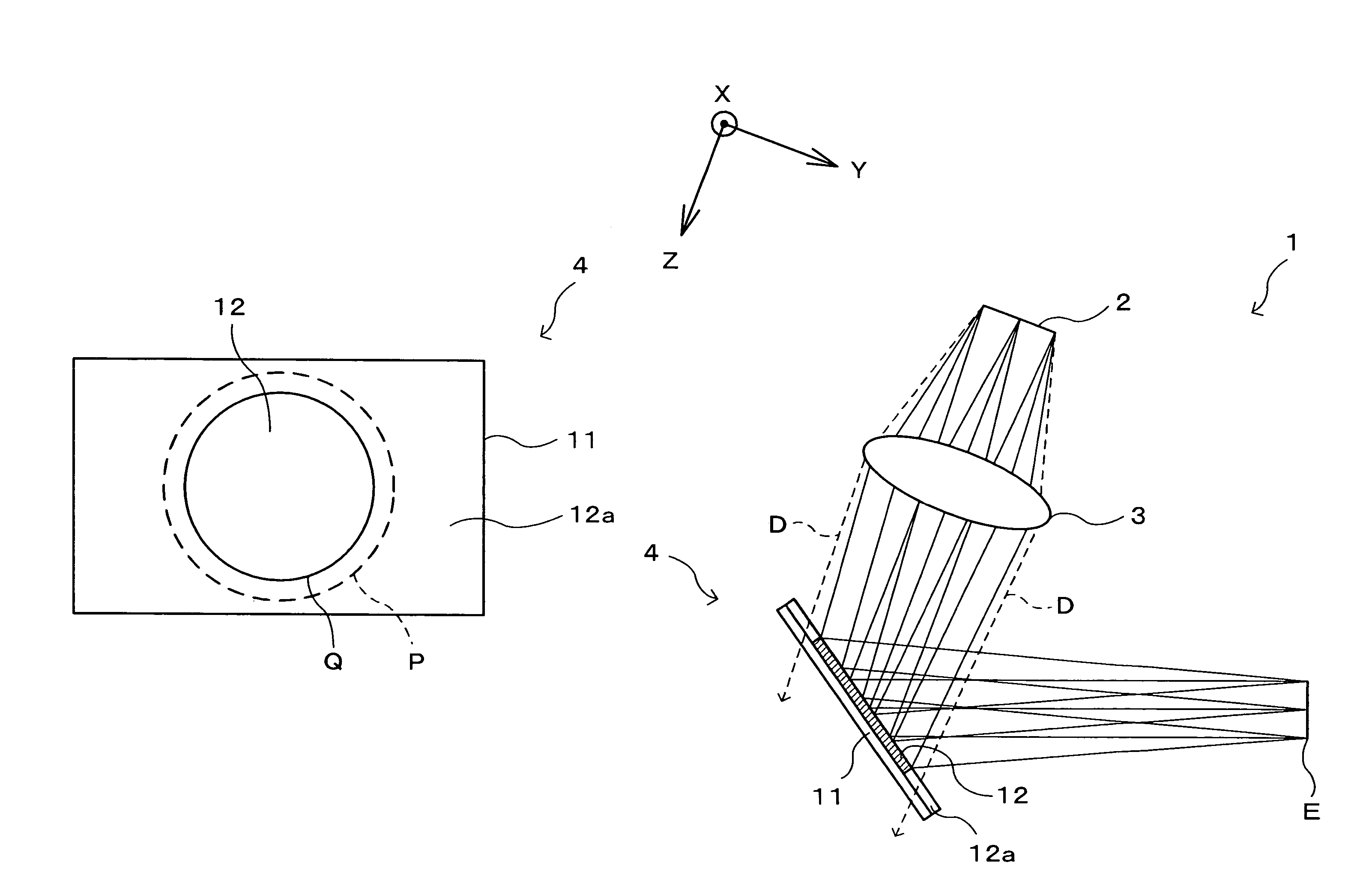
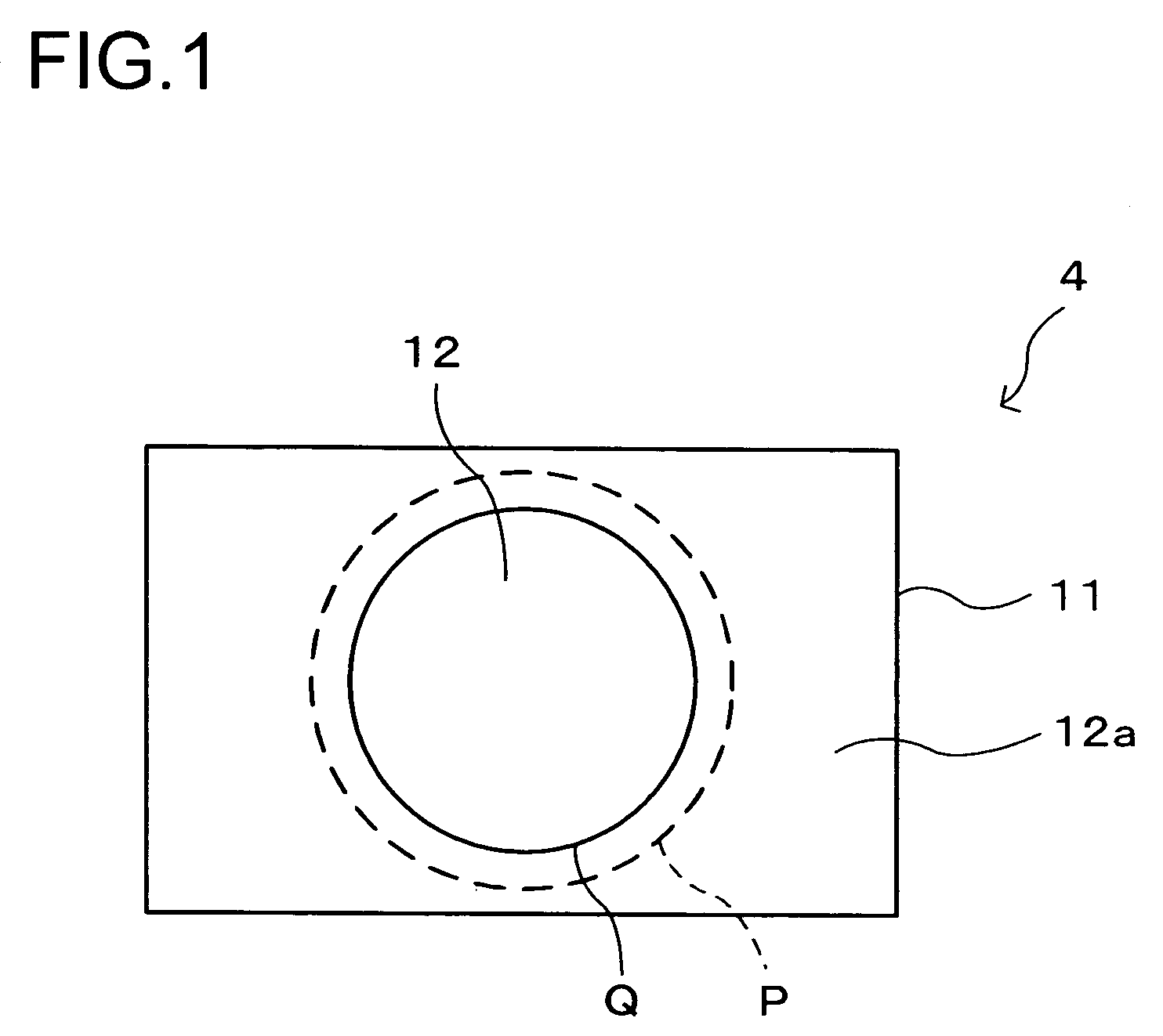
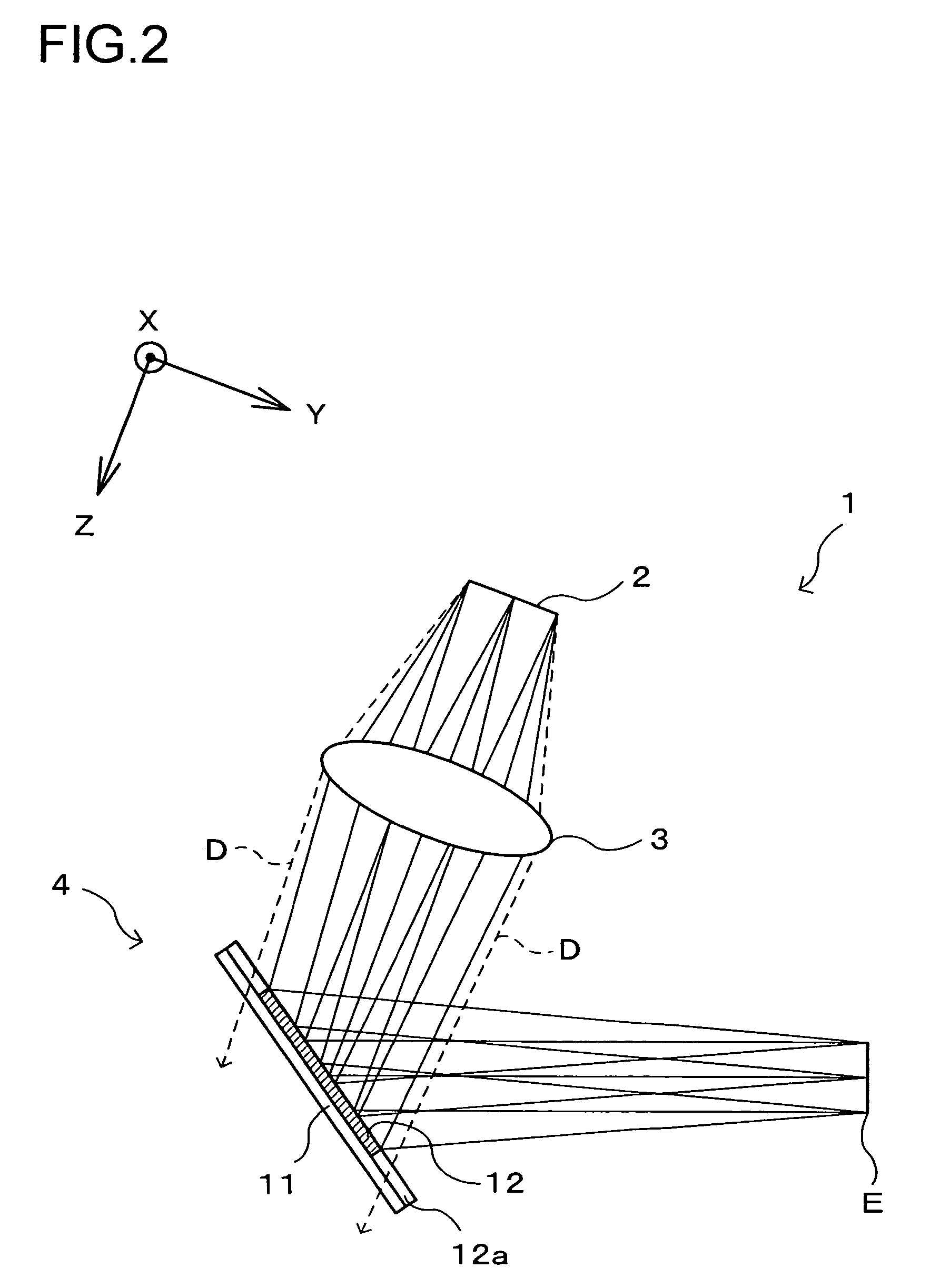
[0056]FIG. 2 is a cross section showing a general structure of the image display device 1 according to this embodiment. This image display device 1 includes a display element 2, an ocular lens 3 and an optical device 4.

[0057]For convenience of description hereinafter, some directions are defined as follows. First, an optical axis is defined as an axis line connecting optically a center of a display area on the display element 2 with a center of an optical pupil E formed by the optical device 4. Then, a Z-direction is defined as a direction of the optical axis of an optical path from the display element 2 to the optical pupil E when it is developed. In addition, an X-direction is defined as a direction perpendicular to an incidence plane of the optical axis to a hologram optical element 12 of the optical device 4 that will ...

second embodiment

[0096]Another embodiment of the present invention will be described as follows with reference to the drawings. For convenience of description, the same elements as in the structure of the first embodiment are denoted by the same reference numerals, and descriptions thereof will be omitted.

[0097](2-1. Structure of the Image Display Device)

[0098]FIG. 10 is a cross section showing a general structure of an image display device 1 according to the second embodiment, and FIG. 11 is an explanatory diagram showing an optical path in the image display device 1 in the state developed optically in one direction. This image display device 1 includes a display element 2 and an optical device 4.

[0099]The display element 2 includes a light source 13, a condensing lens 14 and a light modulation element 15. The light source 13 emits light that is supplied to the light modulation element 15. In this embodiment, particularly, the light source 13 is made up of a white color light source (a white color ...

third embodiment

[0127]Still another embodiment of the present invention will be described as follows with reference to the drawings. For convenience of description, the same elements as in the structure of the first or the second embodiment are denoted by the same reference numerals, and descriptions thereof will be omitted.

[0128](3-1. Structure of the Image Display Device)

[0129]FIG. 14 is a cross section showing a general structure of an image display device 1 according to this embodiment, and FIG. 15 is an explanatory diagram showing an optical path in the image display device 1 in the state developed optically in one direction. This image display device 1 includes a display element 2 and an optical device 4, and structures of the display element 2 and the optical device 4 are slightly different from those in the second embodiment.

[0130]The display element 2 includes a light source 13, a one-way diffuser plate 20, a condensing lens 14 and a light modulation element 15.

[0131]In this embodiment, th...


PUM


Abstract

A hologram optical element is formed on a substrate so as to make an optical device. The hologram optical element is formed in an area smaller than an irradiation area of a beam for reproduction such as image light or object light on the substrate. Supposing that the beam for reproduction is made of a center beam having intensity higher than 50% of center intensity and other peripheral beam, the hologram optical element is formed on the substrate in a size for diffracting only the center beam so that a flare or a ghost can be relieved without using additional optical elements such as a shading plate.

Description

[0001]This application is based on Japanese Patent Application No. 2005-213823 filed on Jul. 25, 2005, the entire contents of which are hereby incorporated by reference.BACKGROUND OF THE INVENTION[0002]1. Field of the Invention[0003]The present invention relates to an optical device including a volume phase type hologram optical element formed on a substrate, an image display device that utilizes the optical device and a head mounted display (hereinafter also referred to as an HMD) equipped with the image display device.[0004]2. Description of Related Art[0005]Conventionally, there are proposed various types of image display devices that conducts image light from a display element (e.g., a liquid crystal display element) to the observer's pupil (of the eye) via an ocular optical system. In this image display device, the image light or external light may propagate through an optical path other than a regular optical path inside the ocular optical system and reach the observer's pupil...

Claims


Application Information

Patent Timeline
Patent Type & Authority Patents(United States)
IPC IPC(8): G03H1/00
CPCG02B5/32G02B27/0172G02B6/00G02B2027/012G02B2027/0132G02B2027/0174G02B2027/0178
Inventor TANIJIRI, YASUSHISHIMIZU, YOSHIENODA, TETSUYAKASAI, ICHIRO
Owner KONICA MINOLTA PHOTO IMAGING
Why Eureka
Try Eureka