Microphone manufacturing method
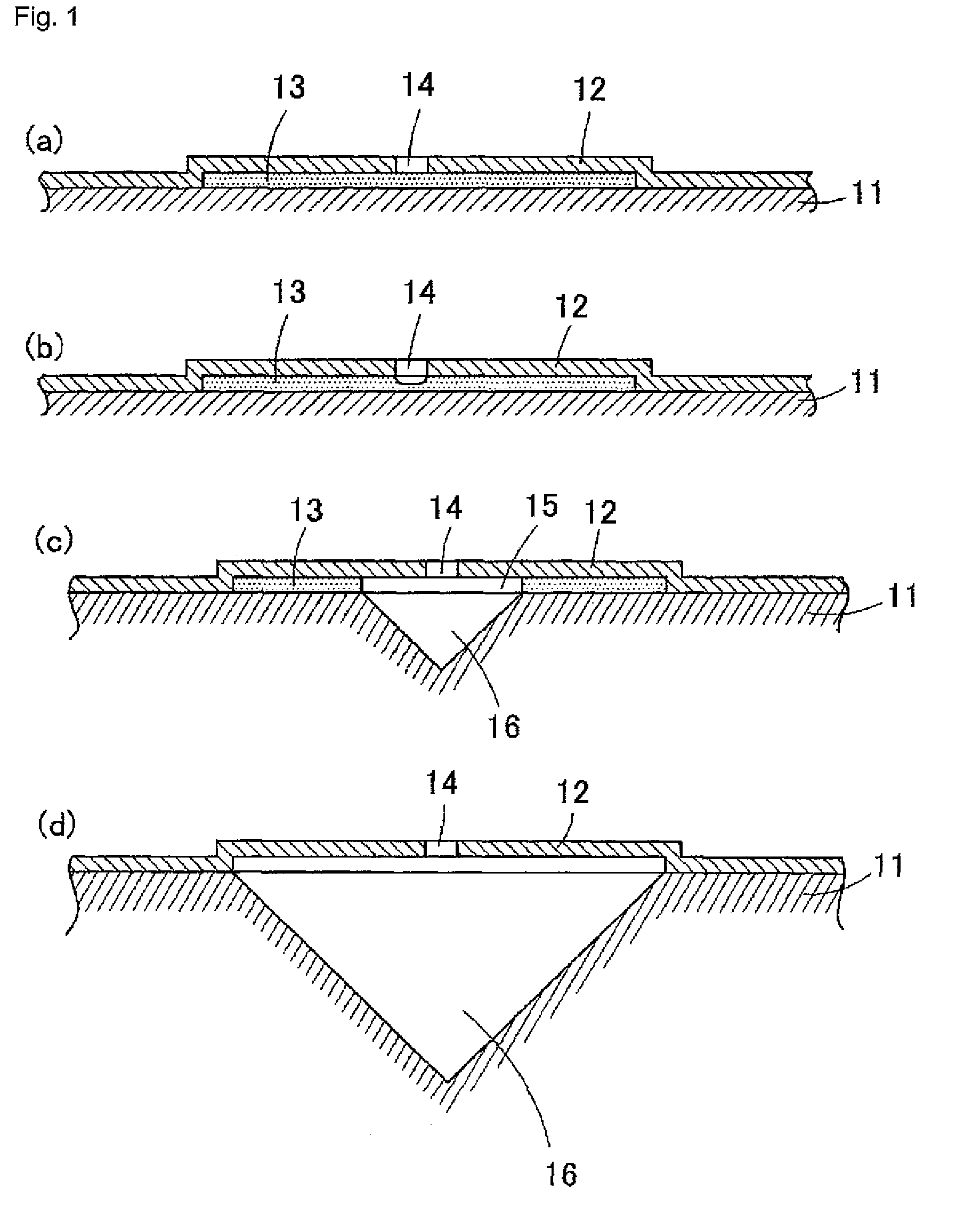
a manufacturing method and microphone technology, applied in the direction of magnets, semiconductor electrostatic transducers, magnetic bodies, etc., can solve the problems of reducing the strength reducing the sensitivity of the vibration film, so as to achieve the effect of easy formation of a bent hole and great acoustic resistan
- Summary
- Abstract
- Description
- Claims
- Application Information
AI Technical Summary
Benefits of technology
Problems solved by technology
Method used
Image
Examples
embodiment 1
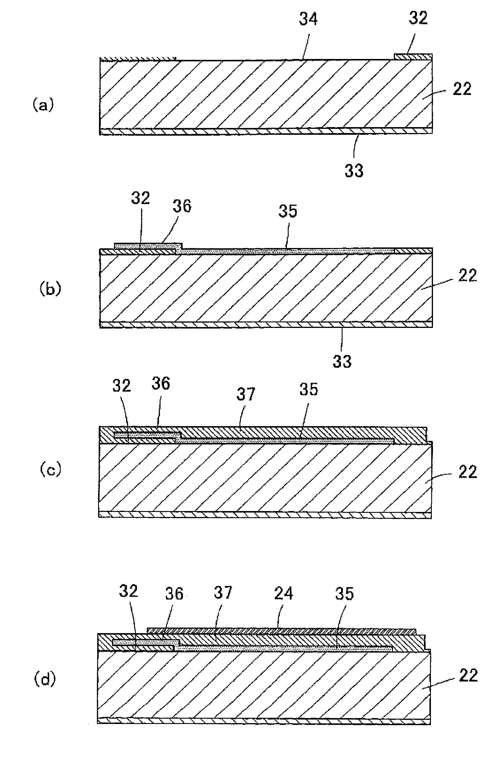
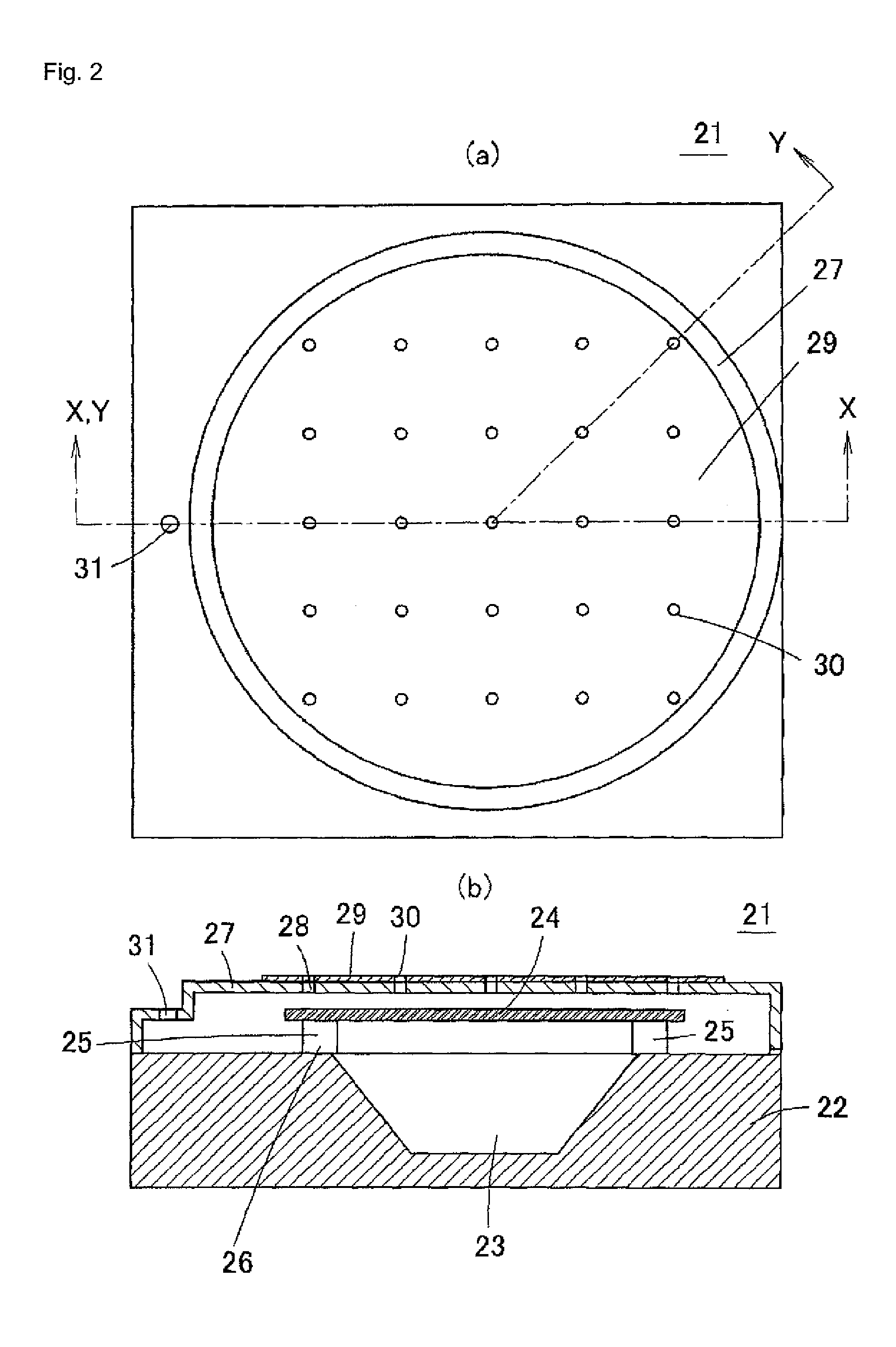
[0062]FIG. 2(a) is a plan view that shows a structure of a microphone 21 in accordance with embodiment 1 of the present invention, and FIG. 2(b) is an X-X line cross-sectional view of FIG. 2(a). Moreover, FIG. 3 is a plan view that shows a microphone 21 from which a back plate has been removed.
[0063]In the microphone 21, a cavity 23 is formed on the surface side of a (100) plane or a (110) plane of the Si substrate 22, and a vibration film 24 is disposed on the Si substrate 22 in such a manner to cover the cavity 23. The cavity 23 is formed by performing crystal anisotropic etching from the surface side of the Si substrate 22, and the peripheral face is formed into a slanting face made of a (111) crystal plane or a crystal plane equivalent thereto, with the opening on the surface side of the cavity 23 being made wider than the bottom face thereof. Four corners of the vibration film 24 are supported by supporting posts 25 formed on the upper surface of the Si substrate 22, with a ben...
embodiment 2
[0097]FIGS. 10(a) to 10(c), FIGS. 11(a) to 11(c) and FIGS. 12(a) to 12(c) are cross-sectional views that show manufacturing processes of a microphone 41 in accordance with embodiment 2 of the present invention. A microphone 41, obtained through these manufacturing processes, makes it possible to eliminate the necessity of a protective film for protecting the vibration film 24 from an etchant upon etching the sacrifice layers 35 and 36 as well as the Si substrate 22; therefore, the film-forming process for the microphone 41 can be simplified. The following description will discuss the manufacturing process thereof.
[0098]First, as shown in FIG. 10(a), a vibration film supporting layer 42 (etching protective film) and a protective film 43, made from SiN, are formed on the surface and the back face of a (100) plane or a (110) plane of an Si substrate 22 (wafer). Next, on the surface of the Si substrate 22, the vibration film supporting layer 42 on an area where a cavity 23 is to be form...
embodiment 3
[0110]FIG. 13(a) is a plan view that shows a structure of a microphone 51 in accordance with embodiment 3 of the present invention, and FIG. 13(b) is a Z-Z line cross-sectional view of FIG. 13(a). This microphone 51 is characterized by adding a functional unit, such as a wrinkle (crease) structure and a stopper 52, to the vibration film 24.
[0111]The wrinkle structure of the vibration film 24 is formed by a bent portion 53 having a square ring shape. The bent portion 53 is bent so as to protrude toward the upper face side of the vibration film 24 in its cross section. By forming this wrinkle structure in the vibration film 24 in this manner, the positional change of the vibration film 24 is increased and the deflection due to a stress is reduced, and these facts are reported by “The fabrication and use of micromachined corrugated silicon diaphragms” (J. H. Jerman, Sensors and Actuators A21-A23 pp. 998-992, 1992).
[0112]The stopper 52 is formed by allowing the surface of the vibration ...
PUM
| Property | Measurement | Unit |
|---|---|---|
| area | aaaaa | aaaaa |
| static pressure | aaaaa | aaaaa |
| static pressures | aaaaa | aaaaa |
Abstract
Description
Claims
Application Information


