Supercharge Your Innovation With Domain-Expert AI Agents!

Method for making GaN-based high electron mobility transistor

a high electron mobility, transistor technology, applied in the field of transistors, can solve the problems high drain bias, low discharge current reduction at high frequencies, and conventionally limited high drain biases of low breakdown voltage, so as to improve carrier confinement and reduce contact and source/drain resistance

Inactive Publication Date: 2010-12-14
LOCKHEED MARTIN CORP
View PDF42 Cites 17 Cited by
  • Summary
  • Abstract
  • Description
  • Claims
  • Application Information

AI Technical Summary

Benefits of technology

[0005]A high electron mobility transistor including: a GaN material system based heterostructure; barrier surface protection during MESA processing; a front end passivating dielectric layer over the heterostructure and defining a plurality of low damage etch processed openings for electrical ohmic contacts for source and drain electrodes and for Schottky contacts for gate electrodes on the heterostructure through the openings; ohmic contact opening surface treatments and source / drain ion implantation to reduce contact and source / drain resistance; and a double heterostructure for improved carrier confinement.

Problems solved by technology

However, drain current reduction at high frequencies has conventionally limited the available output power in GaN material system-based HEMT devices, which is believed to be caused by the surface states.
Low breakdown voltage has conventionally limited high drain biases for GaN material system based HEMT devices.
Further, the power performance of conventional GaN material system based HEMT devices typically degrades at high junction temperatures, due to reduced carrier saturation velocity and increased parasitic resistance.
Repeatable low contact resistance in conventional GaN material system based HEMT devices has also proven problematic for high frequency operation.

Method used


Image

  • Method for making GaN-based high electron mobility transistor
  • Method for making GaN-based high electron mobility transistor
  • Method for making GaN-based high electron mobility transistor

Examples


Embodiment Construction

[0020]It is to be understood that the figures and descriptions of the present invention have been simplified to illustrate elements that are relevant for a clear understanding of the present invention, while eliminating, for the purpose of clarity, many other elements found in typical transistor systems and processing methods. Those of ordinary skill in the art may recognize that other elements and / or steps are desirable and / or required in implementing the present invention. However, because such elements and steps are well known in the art, and because they do not facilitate a better understanding of the present invention, a discussion of such elements and steps is not provided herein.

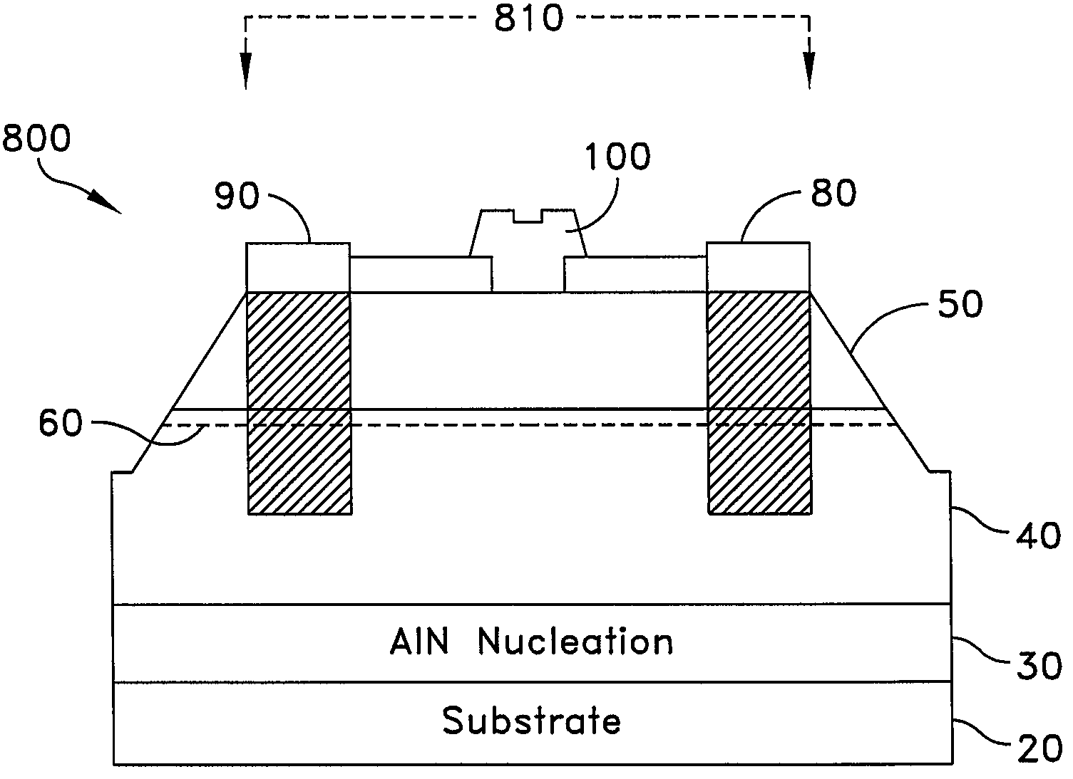
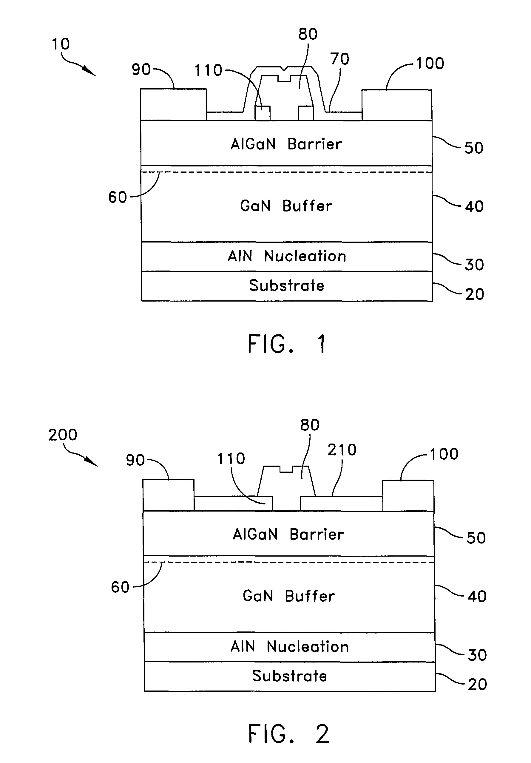
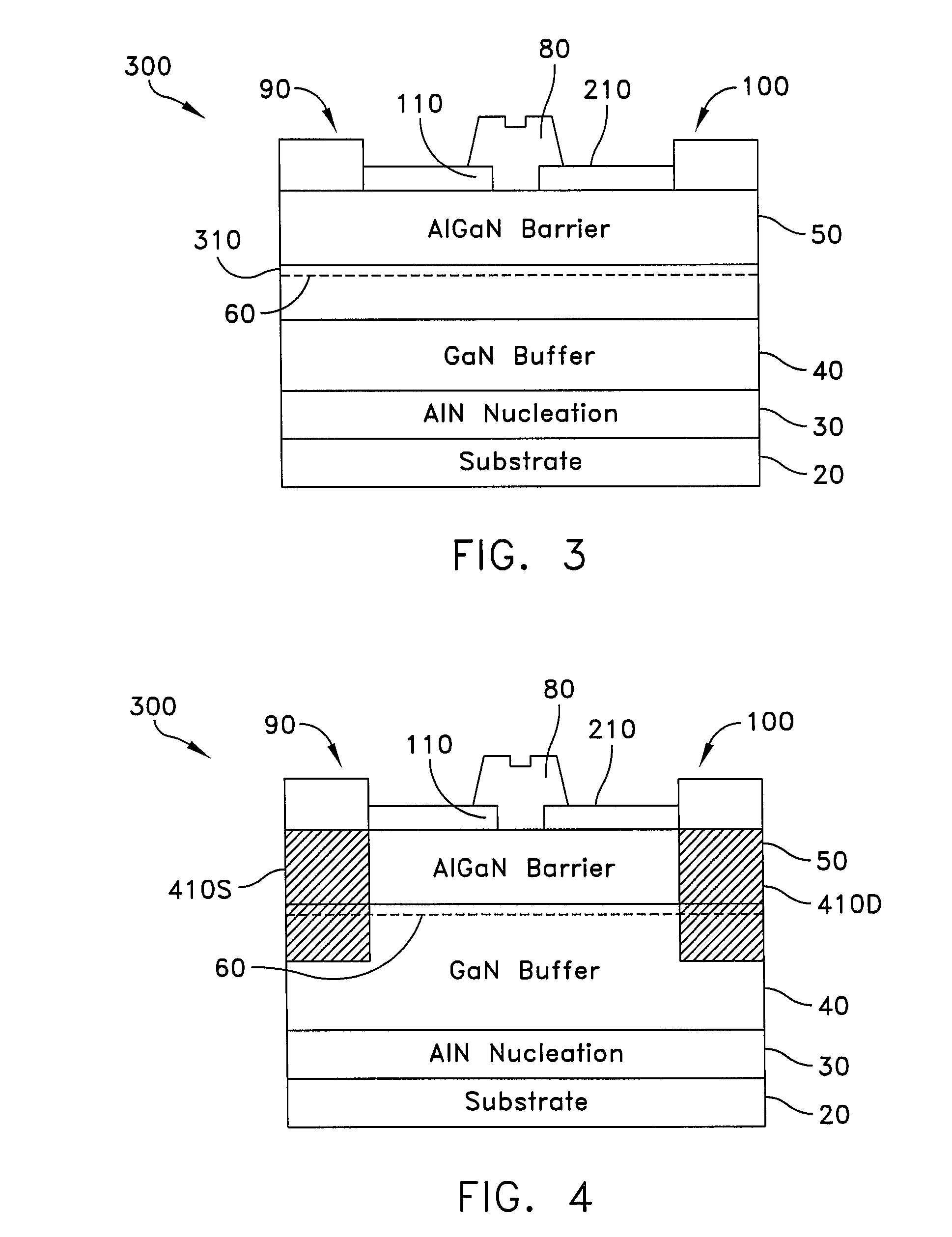
[0021]Referring now to FIG. 1, there is shown a diagrammatic view of a High Electron Mobility Transistor (HEMT) device 10. Device 10 generally includes a substrate 20, an optional nucleation layer 30, buffer layer 40, barrier layer 50, 2 DEG region 60, and passivation layer 70. Device 10 also includes...


PUM


Abstract

A high electron mobility transistor including: a GaN material system based heterostructure; a passivating nitride layer over the heterostructure and defining a plurality of openings; and a plurality of electrical contacts for the heterostructure and formed through the openings.

Description

[0001]This application is a divisional application of copending U.S. patent application Ser. No. 11 / 100,672, entitled GaN-BASED HIGH ELECTRON MOBILITY TRANSISTOR AND METHOD FOR MAKING THE SAME, filed on Apr. 7, 2005, the entire disclosure of which is hereby incorporated as if being set forth in its entirety herein.FIELD OF INVENTION[0002]The present invention relates generally to transistors, and more particularly, to GaN based High Electron Mobility Transistors (HEMTs) and methods for making such transistors.BACKGROUND[0003]High Electron Mobility Transistors are known to be desirable in certain applications. One such application is microwave amplifiers. They are known to generally yield higher output power densities, lower noise figures, and be able to operate at higher frequencies as compared to other Field Effect Transistors (FETs). GaN material system based HEMT's are believed to be desirable for use in Radio Frequency (RF) modulation schemes and interfaces.[0004]However, drain ...

Claims


Application Information

Patent Timeline
Patent Type & Authority Patents(United States)
IPC IPC(8): H01L21/338
CPCH01L29/66462H01L29/7783H01L29/7787H01L29/2003
Inventor ZHANG, AN-PINGKRETCHMER, JAMESKAMINSKY, JR., EDMUND
Owner LOCKHEED MARTIN CORP
Features
  • R&D
  • Intellectual Property
  • Life Sciences
  • Materials
  • Tech Scout
  • Unparalleled Data Quality
  • Higher Quality Content
  • 60% Fewer Hallucinations
Learn More