Semiconductor device and manufacturing method thereof

a technology of semiconductor devices and manufacturing methods, applied in semiconductor devices, semiconductor/solid-state device details, electrical apparatus, etc., can solve problems such as inability to meet the needs of other semiconductor devices, and inability to achieve the same problems as other semiconductor devices, so as to increase the formation margin of the fourth contact electrode and increase the integration

Inactive Publication Date: 2010-12-14
LONGITUDE SEMICON S A R L
View PDF13 Cites 14 Cited by
  • Summary
  • Abstract
  • Description
  • Claims
  • Application Information

AI Technical Summary

Benefits of technology

[0016]According to the present invention, side surfaces of the wiring pattern along an extending direction of the wiring pattern coincide with side surfaces of the third contact electrode. Therefore, the third contact electrode and the fourth contact electrode are not directly short-circuited. Consequently, in forming the fourth contact electrode, it is sufficient to secure a margin for the wiring pattern. As a result, a formation margin of the fourth contact electrode can be increased.
[0017]Such a configuration can be obtained by removing the third contact electrode at a part not covered by the wiring pattern, by etching the third contact electrode by using a mask used to pattern the wiring pattern as it is, as described above. According to this, the third contact electrode is formed in self-aligned with the wiring pattern. Therefore, the wiring pattern and the side surfaces of the third contact electrode can be securely coincided with each other.
[0018]Accordingly, by applying the present invention to a semiconductor memory such as a DRAM, integration can be increased more than that achieved by conventional techniques.

Problems solved by technology

Because these steps are performed separately, misalignment inescapably occurs between the steps.
While conventional problems have been explained above by taking a memory cell of a DRAM as an example, these problems can similarly occur to other semiconductor devices.

Method used


Image

  • Semiconductor device and manufacturing method thereof
  • Semiconductor device and manufacturing method thereof
  • Semiconductor device and manufacturing method thereof

Examples


Embodiment Construction

[0034]Preferred embodiments of the present invention will be explained below in detail with reference to the accompanying drawings.

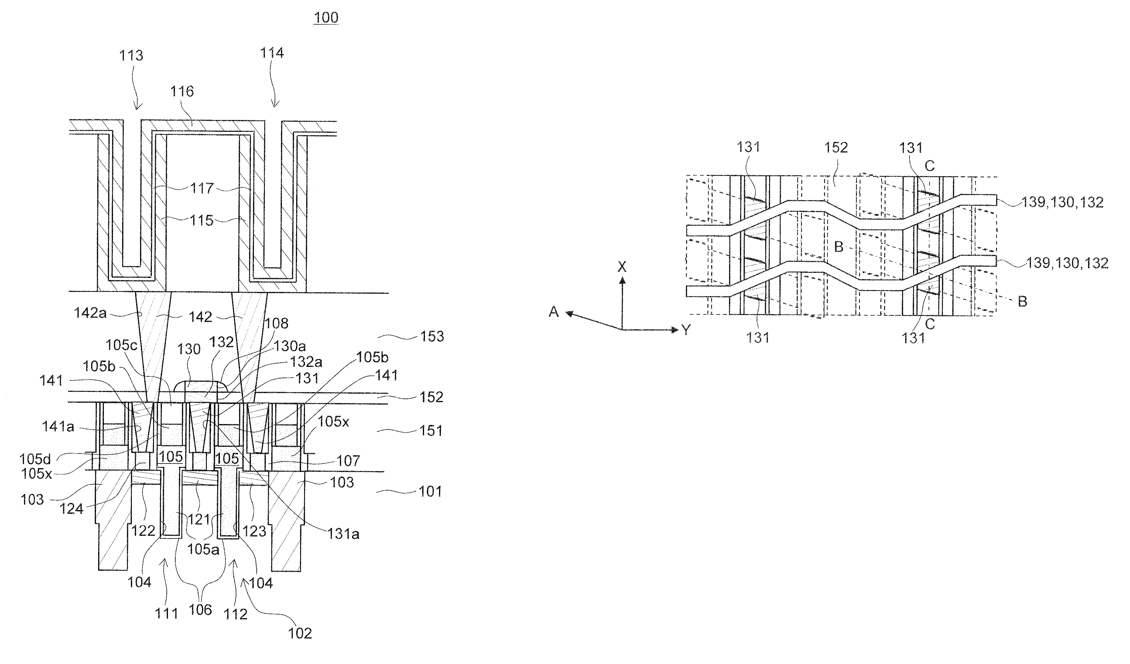
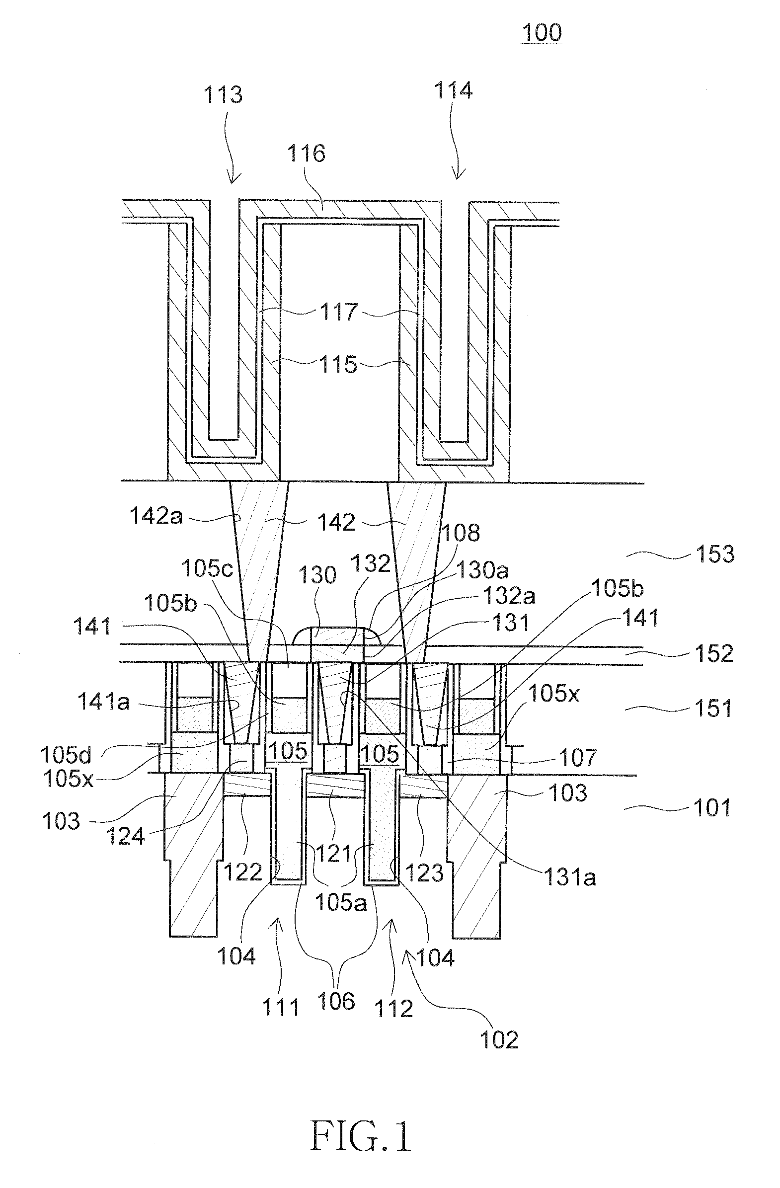
[0035]FIG. 1 is a schematic cross-sectional view showing a configuration of a semiconductor device 100 according to an embodiment of the present invention, and shows a cross section substantially perpendicular to an extending direction of a bit line 130. The semiconductor device 100 according to the present, embodiment is a DRAM, and FIG. 1 shows a partially enlarged memory region of the DRAM.

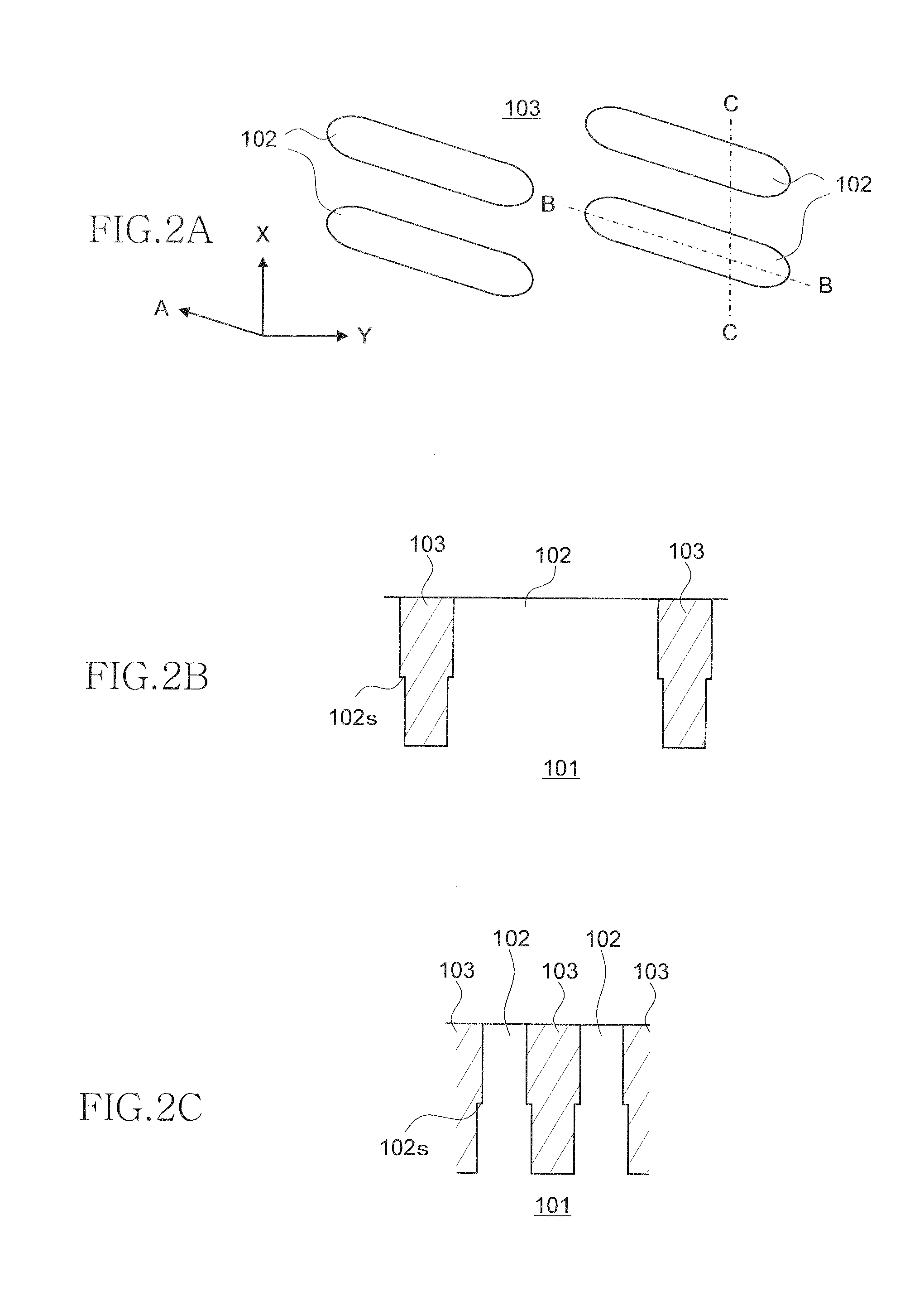
[0036]As shown in FIG. 1, the semiconductor device 100 according to the present embodiment includes cell transistors 111 and 112, and cell capacitors 113 and 114. The cell transistors 111 and 112 are formed in active regions 102 provided on a semiconductor substrate 101. Each active region 102 is a region isolated by an STI (Shallow Trench Isolation) region 103. The cell capacitors 113 and 114 include a lower electrode 115, an upper electrode 116, and a capacitance ...


PUM


Abstract

A semiconductor device includes: a transistor having source and drain regions; first and second contact electrodes embedded in a first interlayer insulating film, and electrically connected to the source region and the drain region, respectively; a third electrode embedded in a second interlayer insulating film positioned in an upper layer of the first interlayer insulating film, and electrically connected to the first contact electrode; a wiring pattern embedded in a third interlayer insulating film positioned in an upper layer of the second interlayer insulating film, and electrically connected to the third contact electrode; and a fourth contact electrode embedded in at least the second and third interlayer insulating films, and electrically connected to the second contact electrode, wherein side surfaces of the wiring pattern along an extending direction of the wiring pattern coincide with side surfaces of the third contact electrode along an extending direction of the wiring pattern.

Description

BACKGROUND OF THE INVENTION[0001]1. Field of the Invention[0002]The present invention relates to a semiconductor device and a method of manufacturing the same, and, more particularly relates to a semiconductor device in which a short circuit between a contact electrode connected to a source region of a transistor and a contact electrode connected to a drain region of the transistor is prevented, and relates to a method of manufacturing the semiconductor device.[0003]2. Description of Related Art[0004]Many transistors are formed on a silicon substrate that constitutes a semiconductor device. Source regions and drain regions of these transistors are connected to wirings and elements on upper layers via various contact electrodes. For example, in a DRAM (Dynamic Random Access Memory) as one of representative semiconductor devices, one of a source region and a drain region of a cell transistor is connected to a bit line, and the other region is connected to a cell capacitor as a memory ...

Claims


Application Information

Patent Timeline
Patent Type & Authority Patents(United States)
IPC IPC(8): H01L23/535H01L21/8242
CPCH01L27/10855H01L27/10888H10B12/485H10B12/0335
Inventor MIKASA, NORIAKI
Owner LONGITUDE SEMICON S A R L
Why Eureka
Try Eureka