Liquid crystal device and projector

a liquid crystal device and projector technology, applied in the field of liquid crystal devices and projectors, can solve the problems of difficulty in sufficiently improving the contrast of liquid crystal devices, and achieve the effect of improving contrast and higher accuracy

Inactive Publication Date: 2011-01-04
SEIKO EPSON CORP
View PDF4 Cites 0 Cited by
  • Summary
  • Abstract
  • Description
  • Claims
  • Application Information

AI Technical Summary

Benefits of technology

[0011]The phase plate has the first substrate, and the inorganic film formed on the first substrate, the inorganic film being formed by supplying the inorganic material obliquely with respect to the substrate surface of the first substrate. The inorganic film is formed on the substrate surface by supplying an inorganic material, such as Ta2O5, obliquely with respect to the substrate surface of each substrate. More specifically, as a method of forming an inorganic film, for example, oblique deposition or sputtering, in which an inorganic material is supplied obliquely in the form of atoms, may be used. When viewed microscopically, the inorganic film has a film structure in which an inorganic material is grown obliquely. With this inorganic film, anisotropy is produced in the refraction index in accordance with the film structure of the inorganic film, and thus the phase of light incident on the phase plate can be compensated.
[0040]In particular, with this to the phase plate, with respect to the variation of the ratio, the ratio of the first phase difference and the second phase difference can be increased, as compared with the ratio of the front phase difference and the first phase difference. Therefore, a phase plate capable of increasing the allowable range of the ratio and improving the contrast can be simply manufactured in terms of quality management.

Problems solved by technology

However, according to the technology disclosed in JP-A-2004-102200 and JP-A-2006-119444, it is technically difficult to sufficiently improve contrast in the liquid crystal device by a phase plate in which the inorganic film is formed by oblique deposition.

Method used


Image

  • Liquid crystal device and projector
  • Liquid crystal device and projector
  • Liquid crystal device and projector

Examples


embodiment

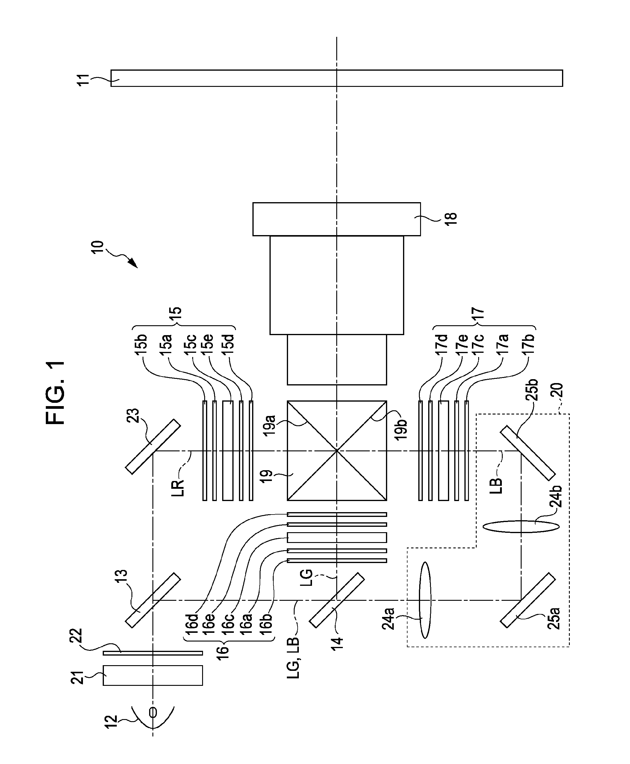
[0058]FIG. 1 is a schematic configuration diagram of a liquid crystal projector according to an embodiment of the invention. A projector 10 is a forward projection-type projector that projects an image onto a screen 11 provided in front. The projector 10 includes a light source 12, dichroic mirrors 13 and 14, liquid crystal light valves 15 to 17, a projection optical system 18, a cross dichroic prism 19, and a relay system 20.

[0059]The light source 12 includes an extra-high pressure mercury lamp that emits light including red, green, and blue light components. The dichroic mirror 13 transmits a red light component LR from the light source 12, and reflects a green light component LG and a blue light component LB. The dichroic mirror 14 transmits the blue light component LB from among the green light component LG and the blue light component LB reflected by the dichroic mirror 13, and reflects the green light component LG. The dichroic mirrors 13 and 14 form a color separation optical...


PUM

PropertyMeasurementUnit
polar angleaaaaaaaaaa
angleaaaaaaaaaa
voltageaaaaaaaaaa

Abstract

A liquid crystal device includes a liquid crystal panel, a pair of polarizers and a phase plate. The phase plate is formed by a supply direction of an inorganic material to the substrate surface set such that a ratio of a front phase difference, which is produced when light is incident along a normal direction of the phase plate, and a first phase difference, which is produced when light is incident along a first direction different from the normal direction, falls within a predetermined range.

Description

BACKGROUND[0001]1. Technical Field[0002]The present invention relates to a liquid crystal device including a polarizer and a phase plate, a projector including a liquid crystal device, and a phase plate for a liquid crystal device.[0003]2. Related Art[0004]As a phase plate for a liquid crystal device, a phase plate is known in which an inorganic film is formed on a substrate by oblique deposition so as to be resistant to light, as compared with an organic film, thereby achieving high lightfastness, (for example, see JP-A-2004-102200 and JP-A-2006-119444).[0005]However, according to the technology disclosed in JP-A-2004-102200 and JP-A-2006-119444, it is technically difficult to sufficiently improve contrast in the liquid crystal device by a phase plate in which the inorganic film is formed by oblique deposition.SUMMARY[0006]An advantage of some aspects of the invention is that it provides a liquid crystal device, which can improve contrast with higher accuracy, a projector including...

Claims


Application Information

Patent Timeline
Patent Type & Authority Patents(United States)
IPC IPC(8): G02F1/1335
CPCG02B27/283G02F1/133632H04N9/3105H04N9/3167H04N9/3197G02F1/133526G02F1/133634G02F1/13454G02F2202/09G02F2413/02
Inventor NINOMIYA, TAKANORISAITO, HIROMI
Owner SEIKO EPSON CORP
Why Eureka
Try Eureka