Scalable processing network for searching and adding in a content addressable memory
a content addressable memory and processing network technology, applied in the field of scalable processing networks, can solve the problems of waste of time and processor cycles in implementation, and achieve the effect of speeding up operation and effectively and efficiently applying
Active Publication Date: 2011-01-04
TELEFON AB LM ERICSSON (PUBL)
View PDF1 Cites 0 Cited by
- Summary
- Abstract
- Description
- Claims
- Application Information
AI Technical Summary
Benefits of technology
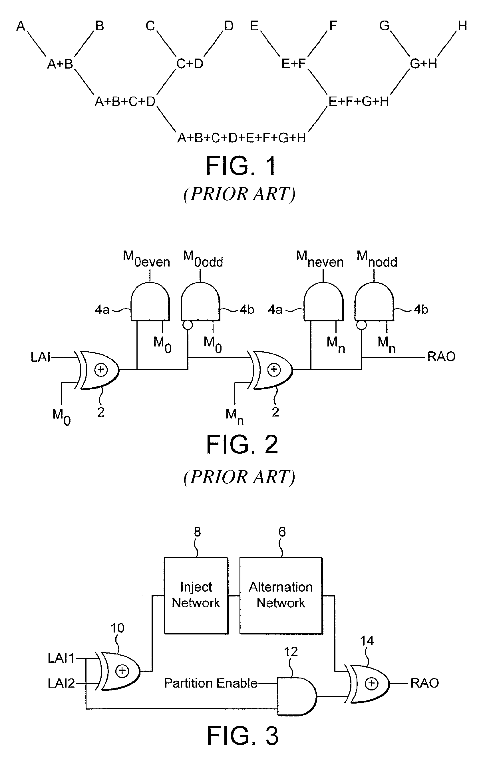
[0009]The versatility of this solution is that it allows the even and odd match sets to be easily generated, offering application flexibility. However, there is a significant drawback namely its very poor speed of execution, which is due to the propagating signal being limited by the gate delay of a single EXOR gate and the number of processors in the string.
[0014]The advantage of this structure is that it enables implementation of a divide and conquer algorithm to be realised in hardware such that massive improvements in speed can be achieved. The speedup is due to the ability to split the matching vector generated by the content addressable memory into odd and even vectors in a few clock cycles and thereafter to iteratively apply the search, and split process to arrive at a single processed element.
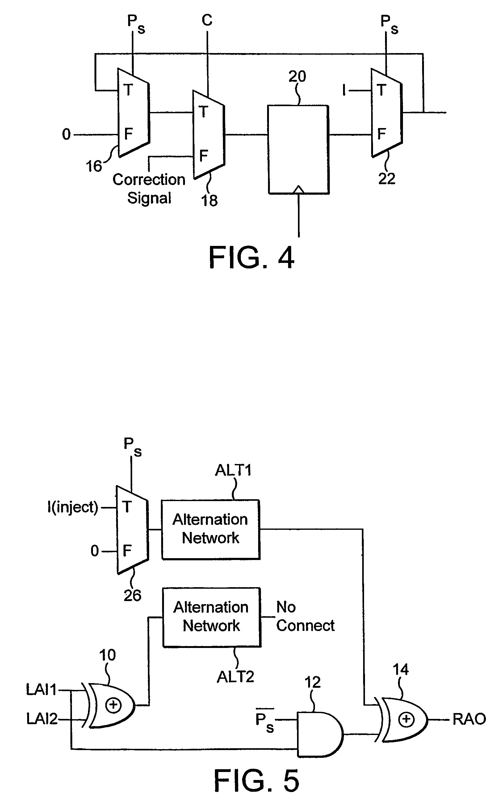
[0017]This communications network supports a search and add process which can be used effectively in a content addressable memory to carry out asynchronous remote addition. It does not matter what the distance is between the different elements that need to be added together, the time taken to implement the addition is the same (in clock cycles). Communication can be effected concurrently which leads to further speed ups and allows the divide and conquer algorithm to be applied effectively and efficiently.
[0018]There is a particular benefit when both the alternation network and the communications network are combined together, the resultant speed up of operation provides a significant advance over the prior art.
[0020]This combination advantageously leads to a compact and relatively fast improved hardware implementation of the desired divide and conquer algorithm.
Problems solved by technology
However, this implementation is wasteful of time and processor cycles.
Method used
View moreImage
Smart ImageViewing Examples
Examples
example i
[0071]Consider the following example. The instruction sequence that needs to be fed to the data processor for a particular application is:
{{A}RepeatSlot(4), B }
where {..} RepeatSlot(N) means repeat the instruction inside the braces N times.
Login to View More PUM
 Abstract
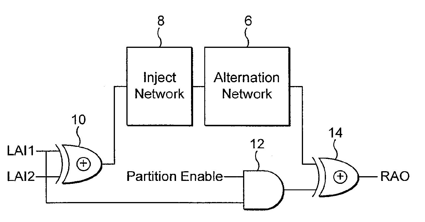
An alternation network for use with a content addressable memory for implementing a divide and conquer algorithm is described. The alternation network comprises: a plurality of alternation modules connected in series together, each module comprising: a plurality of cascaded logic gates arranged to propagate a match parity signal via the gates along at least part of a matching result vector, the matching result vector being generated by execution of a matching instruction on the content addressable memory, and the logic gates being configured to change the parity of the match parity signal in accordance with the matching result vector; and a vector output arranged to output a parity level vector of the propagated match parity signal present at the each gate of the plurality of logic gates; a logic network for dividing the matching result vector into an odd match vector and an even match vector representing respectively odd and even numbered elements of the matching result vector, by use of the parity level vector, and means for writing a selected one of the odd and even match vectors to the content addressable memory.
Description
BACKGROUND OF THE INVENTION[0001]This Invention relates to scalable processing networks, in particular but not restricted to processing networks employing concurrent microprocessor technology used in the communications industry.[0002]A common type of processor function is to locate in a memory store all occurrences of a desired value, and then to determine the sum of all occurrences. Typically this is achieved through a series of synchronous matching actions wherein each memory store location is searched and matched in turn. However, this implementation is wasteful of time and processor cycles.[0003]In a case where a processor has an associated local memory store, for example the multiprocessor implementation of Single Instruction Multiple Data (SIMD) processors which is the subject of the applicant's European Patent published as EP 0983556, the search and summation function as described in the above paragraph may be carried out through a type of inter-processor communication known ...
Claims
Login to View More Application Information
Patent Timeline
 IPC IPC(8): G06F12/00G06F13/00G06F13/28G06F15/80
CPCG06F15/8038
Inventor JALOWIECKI, IANWHITAKER, MARTINLANCASTER, JOHNBOUGHTON, DONALD
Owner TELEFON AB LM ERICSSON (PUBL)


