
Image sensor, module and electronic device

a technology of image sensor and electronic device, which is applied in the direction of instruments, television systems, and details of television system scanning, etc., can solve the problems of signal attenuation, signal attenuation due to long lines, and the original image read by the image sensor cannot be reproduced with precision, so as to achieve accurate information output and expand the dynamic range of signal output.

Inactive Publication Date: 2011-01-11
ROHM CO LTD
View PDF9 Cites 0 Cited by
  • Summary
  • Abstract
  • Description
  • Claims
  • Application Information

AI Technical Summary

Benefits of technology

The solution effectively expands the dynamic range of signal output and ensures accurate information transmission by minimizing signal attenuation and offset voltage effects, while reducing the semiconductor chip area and power consumption.

Problems solved by technology

In this case, even if an image is reproduced based on image signals that are output from the image sensor, the original image read by the image sensor could not be reproduced with precision.
In other words, a problem of signal attenuation occurs.
Therefore, the problem of the signal attenuation due to the long line has not been solved.

Method used


Image

  • Image sensor, module and electronic device
  • Image sensor, module and electronic device
  • Image sensor, module and electronic device

Examples


first embodiment

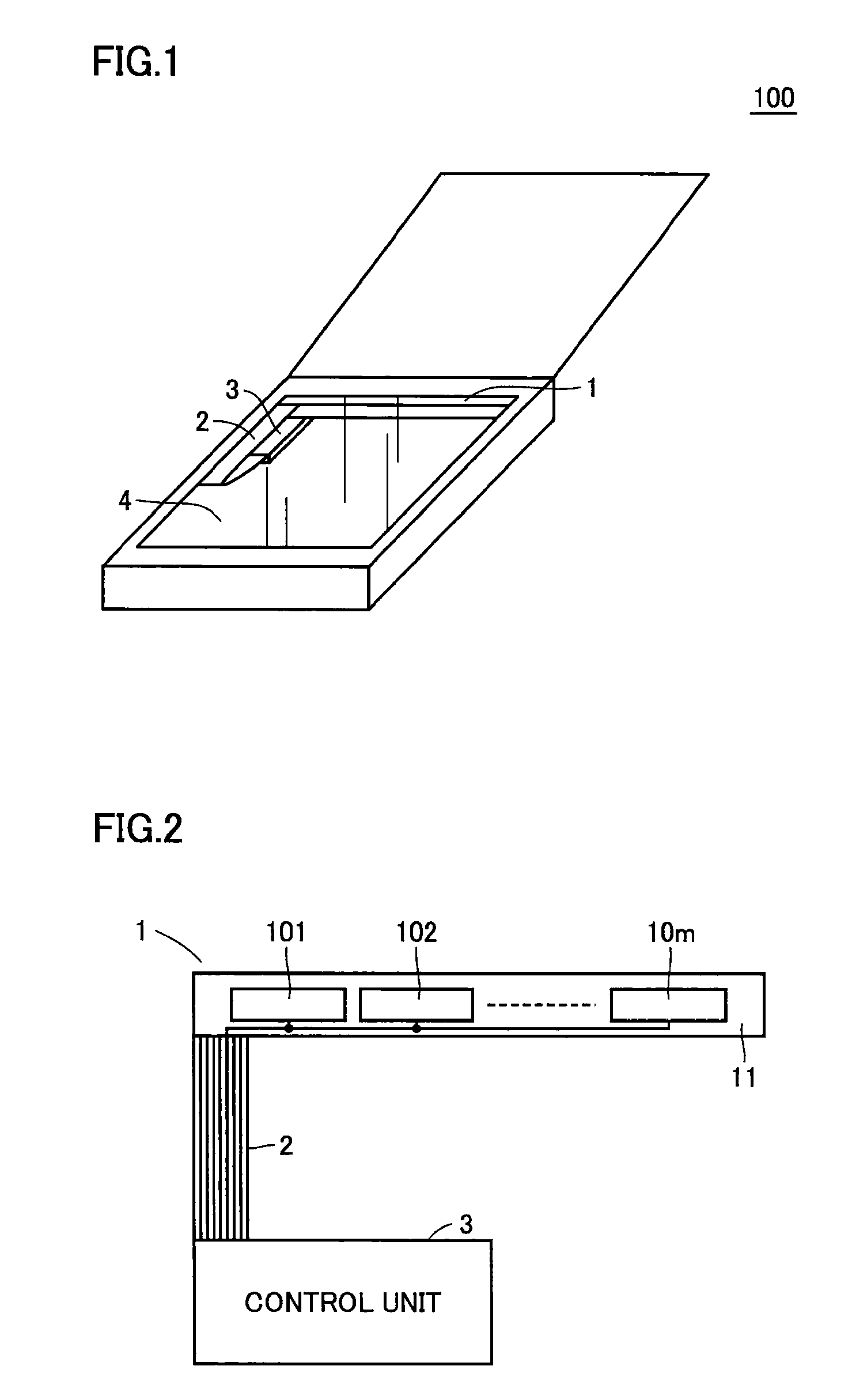
[0040]FIG. 1 is a diagram showing an example of an electronic device on which mounted an image sensor according to the present embodiment.

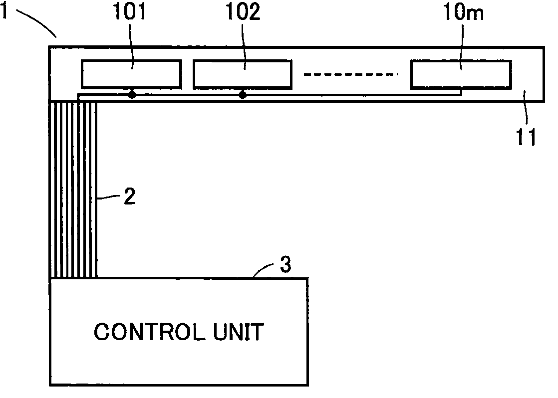
[0041]Referring to FIG. 1, a scanner 100 is an example of the electronic device on which an image sensor of the present embodiment is mounted. Scanner 100 includes an image sensor head 1, a flexible cable 2, a control unit 3 connected through flexible cable 2 to image sensor head 1, and a document reading platform 4 on which an original document where characters and image are indicated is to be placed.

[0042]Image sensor head 1 corresponds to the module of the present invention. Image sensor head 1 is movable, and reads characters and images from the document placed on document reading platform 4 and transmits an image signal to control unit 3.

[0043]Control unit 3 reproduces the image read by image sensor head 1 based on the image signal. Control unit 3 controls operation of image sensor head 1.

[0044]The electronic device on which the image sensor ...

second embodiment

[0095]Regarding an image sensor of a second embodiment, the configuration of the correction circuit can be simplified as compared with the image sensor of the first embodiment.

[0096]FIG. 7 is a diagram showing a configuration of an image sensor of the second embodiment.

[0097]Referring to FIGS. 7 and 3, image sensor 101A differs from image sensor 101 in that the former sensor includes a correction circuit 22A instead of correction circuit 22.

[0098]Correction circuit 22A includes a capacitor 30, a switch SWA, a constant voltage source 34 and a buffer 35. One end of capacitor 30 is connected to a node N0 and the other end of the capacitor is connected to a node N3. One end of switch SWA is connected to node N3 and the other end of switch SWA is connected to a voltage output terminal of constant voltage source 34. The input terminal of buffer 35 is connected to node N3 and the output terminal of buffer 35 is connected to terminal OUT.

[0099]As seen from a comparison between correction ci...


PUM


Abstract

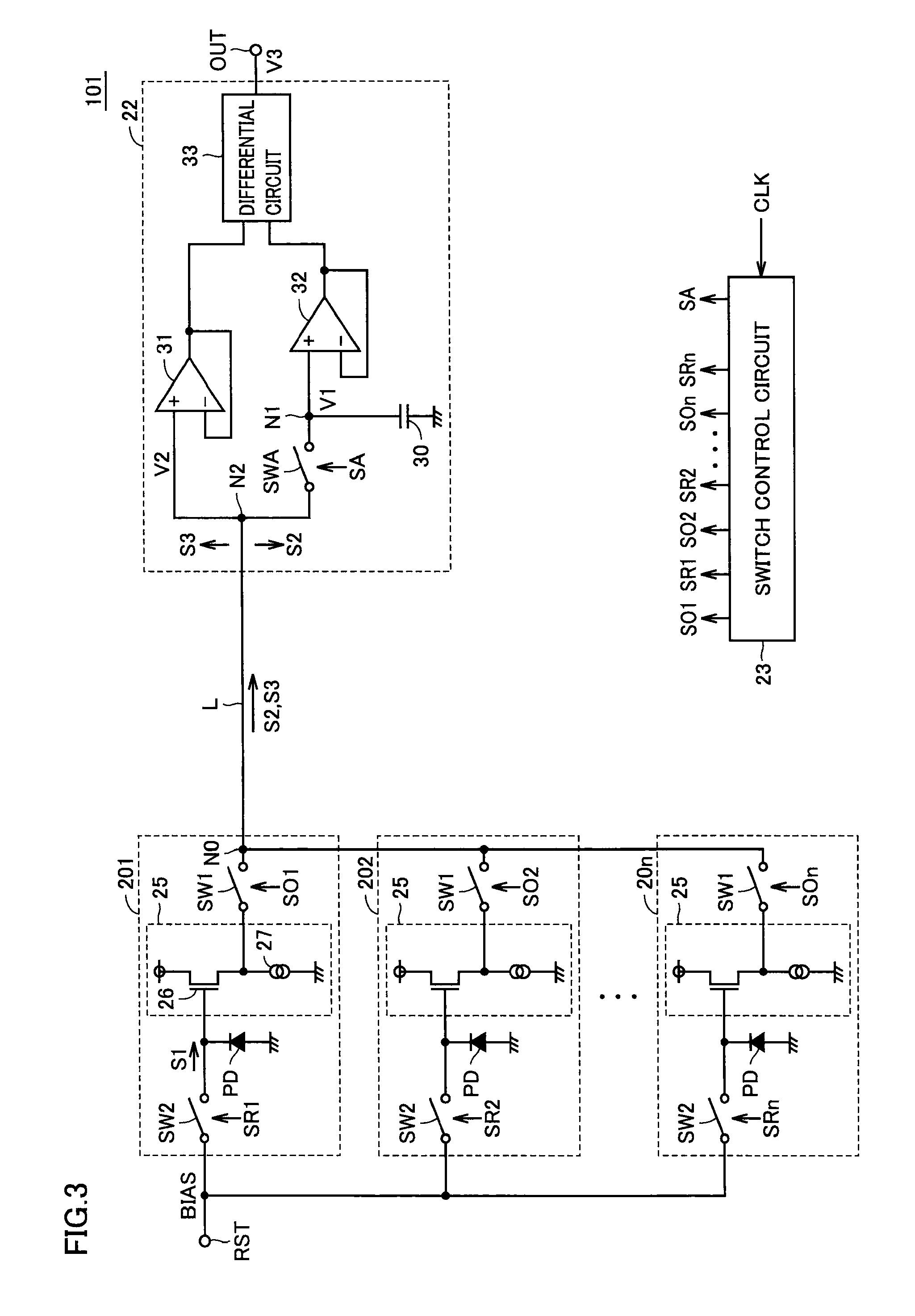
From an amplifier circuit of a plurality of pixels each, a signal is directly output to a signal line. Even if the signal line is longer and the signal line has an increased parasitic capacitance, attenuation of the signal transmitted through the signal line can be prevented. Therefore, the dynamic range of the signal output can be expanded and the information can be output accurately.

Description

BACKGROUND OF THE INVENTION[0001]1. Field of the Invention[0002]The present invention relates to an image sensor, a module and an electronic device including the module. In particular, the invention relates to a linear image sensor used for document reading and for image input for example, a module including a plurality of linear image sensors and an electronic device including the module.[0003]2. Description of the Background Art[0004]A common CMOS (Complementary Metal Oxide Semiconductor) image sensor includes a plurality of photoelectric conversion elements (such as photodiodes for example) for converting an optical signal into an electric signal and a plurality of amplifier circuits provided correspondingly to a plurality of photoelectric conversion elements respectively. The amplifier circuit is configured for example with a source-follower circuit including a MOS transistor.[0005]In the image sensor having the above-described configuration, regardless of whether or not light i...

Claims


Application Information

Patent Timeline
Patent Type & Authority Patents(United States)
IPC IPC(8): H04N1/40G06T1/00H04N1/028
CPCH03F3/08
Inventor MURAKAMI, TAKATOSHIYAMADA, NOBUYUKI
Owner ROHM CO LTD
Learn More