Circuit arrangement and method of testing an application circuit provided in said circuit arrangement

a circuit and circuit technology, applied in the field of integrated circuit arrangements, can solve the problems of high cost, large test vector memory, complex and large scale integration testing systems, etc., and achieve the effects of improving the error coverage of the document u.s., reducing the number of bist hardware, and clear saving surface area

Inactive Publication Date: 2011-01-11
NXP BV
View PDF13 Cites 0 Cited by
  • Summary
  • Abstract
  • Description
  • Claims
  • Application Information

AI Technical Summary

Benefits of technology

[0024]The essential advantage of the present invention is that a clear saving in surface area is made owing to the implementation of the DLBIST hardware based on a ROM compared with the conventional gate-based implementation, so that the additional DLBIST hardware is reduced to an acceptable surface area. The consequence of this area reduction is a clear cost reduction for the integrated circuit with the built-in logic self-test according to the present invention.
[0025]The invention finally relates to the use of at least one integrated circuit arrangement of the kind described above and / or a method of the kind described above for testing at least one application circuit.
[0026]The present invention accordingly relates to the technical field of integrated circuits (ICs), their design for testability (DfT), their computer-aided design (CAD), and their computer-aided testing (CAT); the present invention in particular relates to integrated circuit arrangements with very high integration densities and built-in self-test logic (so-termed BIST logic) for finding production defects in the logic part of the circuit.SHORT

Problems solved by technology

In an external test, however, many production-related problems and high expenses occur owing tothe very high integration density of such integrated circuits,the very high clock frequencies at which these integrated circuits operate, andthe very large number of test vectors required, which lead to complicated Very Large Scale Integration (VLSI) testing systems with large test vector memories.
The test arrangements disclosed in these publications, however, are not suitable inter alia for solving test problems which are caused substantially by high Integrated Circuit (IC) internal clock frequencies and Input Output (I / O) bond pad stages that are very slow in comparison with the former.
The high internal clock frequencies of the integrated circuits have indeed an unfavorable ratio to the comparatively very slow input / output bond pad stages that lead to the exterior.
The conventional implementation based on logic gates of the additional deterministic logic BIST hardware (the so-termed DLBIST hardware) here leads to a too large additional DLBIST hardware in practice with real, large integrated circuit arrangements.

Method used


Image

  • Circuit arrangement and method of testing an application circuit provided in said circuit arrangement
  • Circuit arrangement and method of testing an application circuit provided in said circuit arrangement
  • Circuit arrangement and method of testing an application circuit provided in said circuit arrangement

Examples


Embodiment Construction

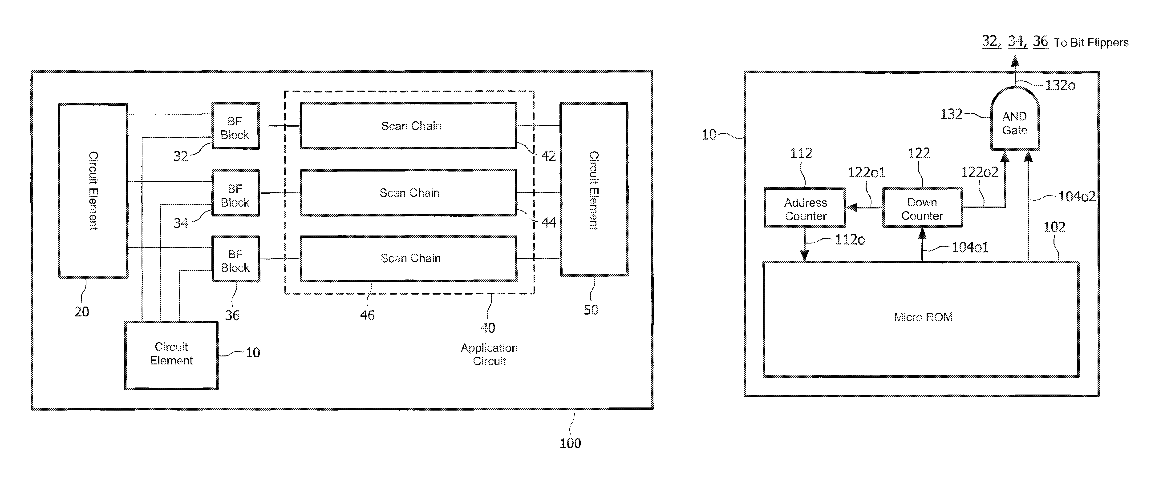
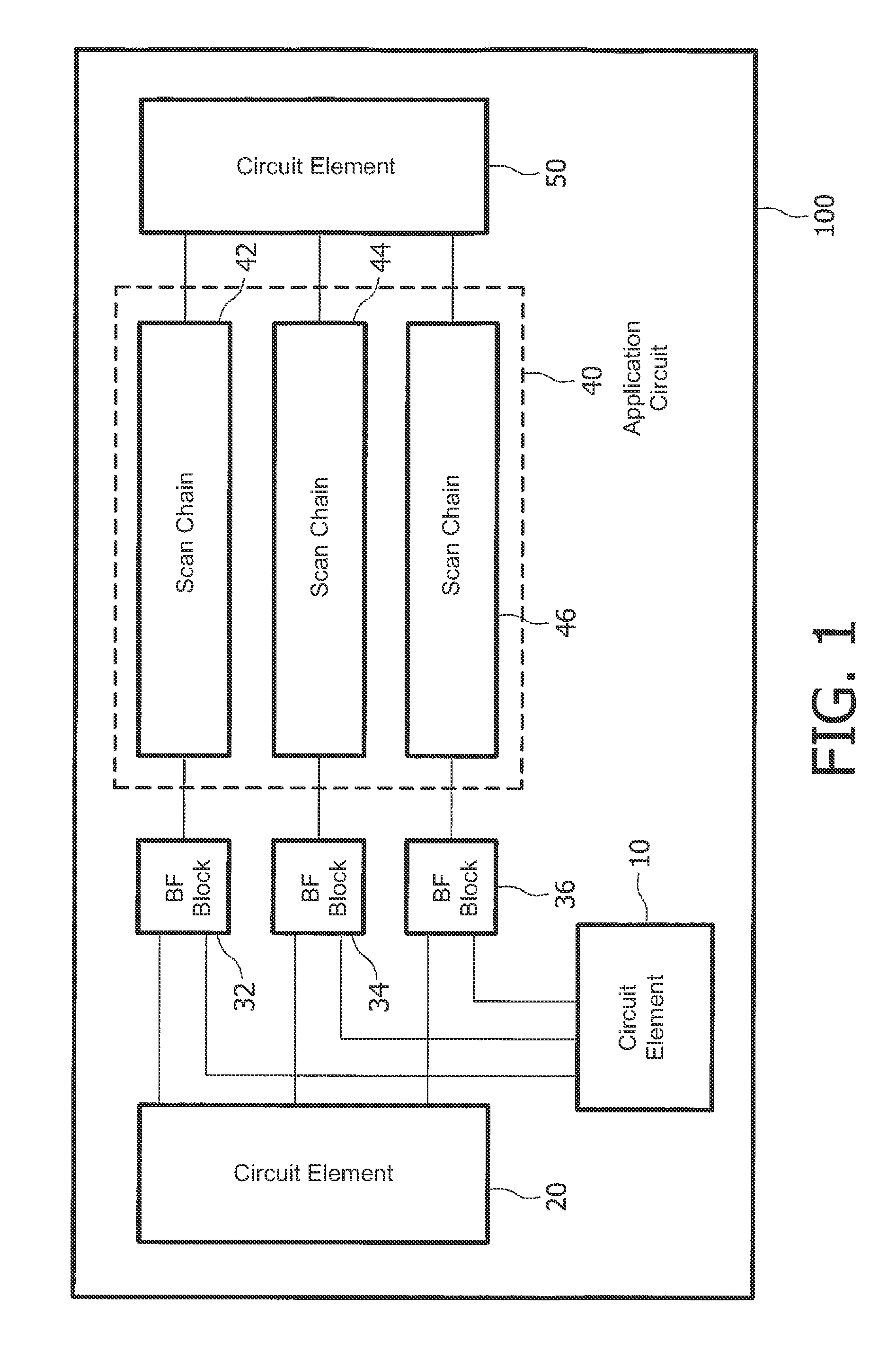
[0033]FIG. 1 is a block diagram of an integrated circuit arrangement (IC) 100 which comprises an application circuit 40. The application circuit 40 is that circuit that is designed for the practical use of the integrated circuit 100.

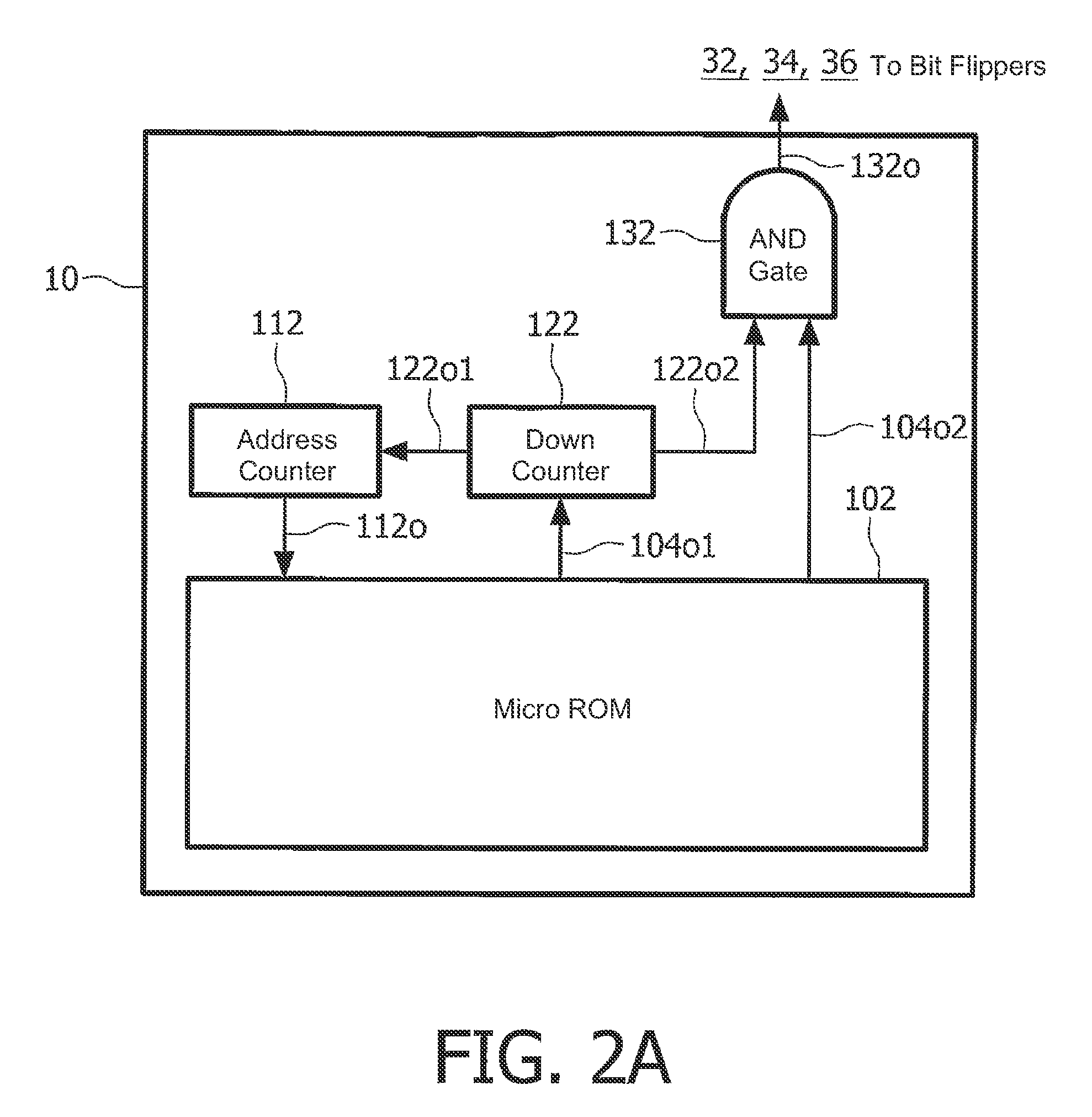
[0034]There is a desire to test the application circuit 40 for perfect operation after manufacture of the IC 100. For this purpose, a self-test circuit is provided on the integrated circuit 100, comprising the circuit elements 10, 20, 32, 34, 36, 50 as shown in FIG. 1.

[0035]In the integrated circuit 100 according to the invention, this self-test circuit is designed such that the associated circuit elements 10, 20, 32, 34, 36, 50 are arranged fully outside the application circuit 40, so that the behavior of the application circuit 40 during normal operation is not influenced by the self-test circuit.

[0036]It is assumed for the embodiment of FIG. 1 that the application circuit 40 comprises two circuit chains (so-termed scan chains with reference numerals 4...


PUM


Abstract

According to an example embodiment, there is an integrated circuit arrangement with at least one application circuit to be tested, and with at least one self-test circuit for testing the application circuit and generating at least one pseudo-random test sample. wherein said The pseudo-random test sample is converted into at least one test vector that is programmable and / or deterministic and is supplied to the application circuit for testing purposes via at least one logic gate and at least one signal that is applied to said logic gate. The output signal arising in dependence on the deterministic test vector is evaluated by the application circuit by at least one signature register. Furthermore, there is a method of testing the application circuit such that Built In Self Test (BIST) hardware connected to the additional deterministic logic is reduced; it is suggested that the signal supplied to the logic gate is made available by a Bit Flipping Function (BFF) logic circuit based on at least one self-test circuit.

Description

FIELD OF THE INVENTION[0001]The invention relates to an integrated circuit arrangement[0002]with at least one application circuit to be tested, and[0003]with at least one self-test circuit provided for testing the application circuit and[0004]generating at least one pseudo-random test sample,[0005]wherein said pseudo-random test sample can be converted into at least one test vector that is programmable and / or deterministic and that can be supplied to the application circuit for testing purposes[0006]via at least one logic gate and[0007]of with at least one signal that can be applied to said logic gate, and[0008]With at least one signature register, the output signal arising in dependence on the deterministic test vector can be evaluated by the application circuit.[0009](cf. prior-art publication DE 102 01 554 A1 which has a US-counterpart publication (application Ser. No. 10 / 501,796) now granted U.S. Pat. No. 7,039,844 B2 dated May 2, 2006).[0010]With at least one self-test circuit,...

Claims


Application Information

Patent Timeline
Patent Type & Authority Patents(United States)
IPC IPC(8): G01R31/28
CPCG01R31/3187
Inventor WITTKE, MICHAELHAPKE, FRIEDRICH
Owner NXP BV
Why Eureka
Try Eureka