

Protective film material for laser processing and wafer processing method using the protective film material
a protective film and laser processing technology, applied in the direction of unsaturated alcohol polymer adhesives, amide/imide polymer adhesives, manufacturing tools, etc., can solve the problems of insufficient removal of debris, complex installation and operation of apparatuses and working conditions, and debris that is also unwantedly attached to the surface of the device, etc., to achieve the effect of easy removal by washing
Active Publication Date: 2020-06-30
NIKKA SEIKO
View PDF7 Cites 0 Cited by
- Summary
- Abstract
- Description
- Claims
- Application Information
AI Technical Summary
Benefits of technology
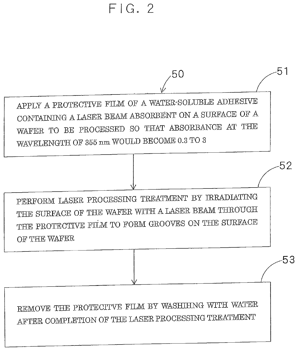
The present invention provides a protective film material for laser processing that can protect both the streets and the central portion of device chips on a wafer surface. After laser processing, the protective film can be easily removed with debris by washing with water, resulting in a clear surface without any attachment of debris. The use of this protective film material can suppress debris formation and scattering, and allow for efficient production of devices. Additionally, the protective film material can be used as a scratch protective film for various articles.
Problems solved by technology
The explosions blast substances (debris) by sublimation from the wafer, and the blasted substances adhere as foreign matter (debris) to the portions adjacent to the processing grooves formed on the streets on the wafer surface, and part of the debris also unwantedly adheres to the surface of the devices as well.
However, these conventional methods require the installation and operation of apparatuses and working conditions thereof are complex.
And, removal of debris has not been sufficiently achieved even with such methods, and improvements have been demanded.
However, these methods are not enough for protection of the device chips since the scattered debris sometimes scatters to the central portion of the device chips away from the streets and fixes thereto, or may sometimes cause burning, scorching or the like by thermal change.
Particularly, for image sensors to be used for cameras, attachment of even a small amount of debris forms stains on the lenses on the surface of the device chips, causing deterioration of performance of the image sensors and an increase in rejection rate, and further improvements to deal with such drawbacks have been demanded.
Method used
View moreImage
Smart ImageViewing Examples

Examples
example 1
[0065]16.2 mass % of PVA, 0.8 mass % of PNVA-1, 1.5 mass % of the laser beam absorbent, 0.6 mass % of TEA, 1.0 mass % of phenyl glycol, 15.0 mass % of PGM and 64.9 mass % (balance) of the pure water were thoroughly mixed to obtain a protective film material for laser processing.
examples 2 to 4
[0066]Protective film materials for laser processing of Examples 2 to 4 were obtained on the basis of the compositions as shown in Table 1 in accordance with the procedure of Example 1.
example 5
[0067]13.1 mass % of PVA, 1.0 mass % of PNVA-2, 1.85 mass % of the laser beam absorbent, 0.75 mass % of TEA, 1.0 mass % of phenyl glycol, 15.0 mass % of PGM and 67.3 mass % (balance) of the pure water were thoroughly mixed to obtain a protective film material for laser processing.
Login to View More PUM
| Property | Measurement | Unit |
|---|---|---|
| pH | aaaaa | aaaaa |
| temperature | aaaaa | aaaaa |
| wavelength | aaaaa | aaaaa |
Abstract
A protective film material for laser processing comprises a solution of a water-soluble adhesive and a water-soluble laser beam absorbent added to adjust absorbance at a wavelength of 355 nm (absorbance as calculated as a 200-times diluted solution) to 0.3 to 3. The protective film effectively absorbs an irradiated laser beam, reduces generation of debris during laser beam irradiation, and can be removed by washing with water after completion of the laser processing treatment, thereby providing reliable processing. The water-soluble adhesive is preferably a blend of polyvinyl alcohol and poly-N-vinyl acetamide, which are preferably blended at a ratio of 100 to 200:1 in terms of amounts of respective components.
Description
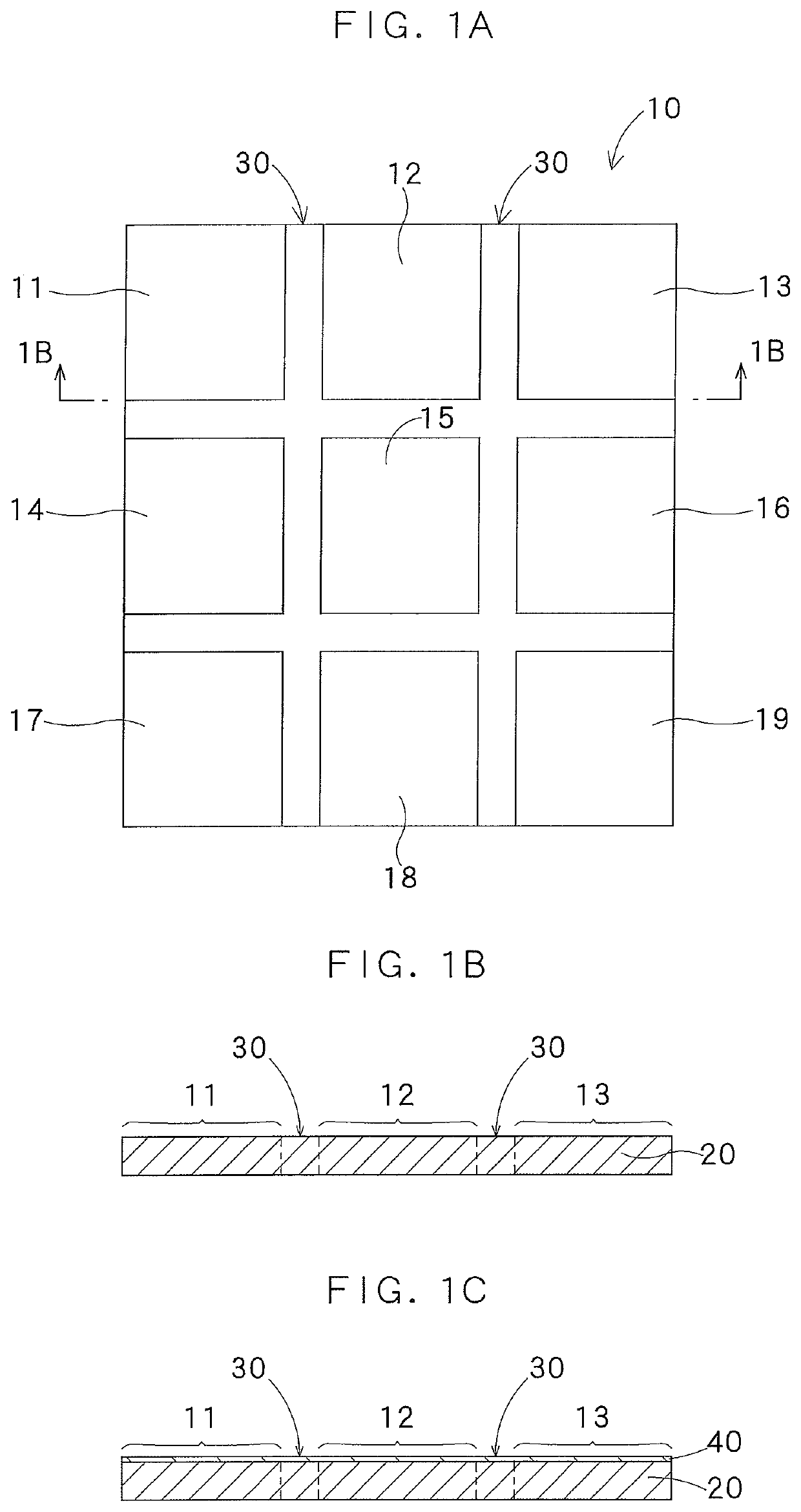
FIELD OF THE INVENTION[0001]The present invention relates to a protective film material that is used to coat the surface of a wafer for protection when the wafer is irradiated with a laser beam to carry out a processing operation such as scribing, dicing or grooving. The present invention also relates to a wafer processing method using the protective film material.BACKGROUND INFORMATION[0002]On wafers provided with patterns such as LSI, CMOS or power devices formed on a substrate made of a compound such as silicon or sapphire, many devices are formed and partitioned by division lines, called scribe streets or simply streets. When the devices separated lengthwise and widthwise by streets are singularized into individual pieces by dividing at the streets, dicing is carried out by a blade or irradiation with a laser beam. The dicing method by a laser beam is one of the effective methods.[0003]When the dicing is carried out by a laser beam, the irradiation of the laser beam causes explo...
Claims
Login to View More Application Information
Patent Timeline
 Patent Type & AuthorityPatents(United States)
IPC IPC(8): H01L23/00H01L21/78B23K26/40H01L21/67H01L21/268B23K26/18B23K101/40
CPCH01L23/562H01L21/268H01L21/6715B23K26/18B23K26/40H01L21/78B23K2101/40B23K26/364B23K26/009C09J129/04C09J11/00C09J133/26C09D129/04C09D133/26C09D7/40
InventorTADANO, TSUYOSHIHIROSE, MASAFUMITOMITA, DAISUKE
OwnerNIKKA SEIKO