Semiconductor device

a semiconductor device and semiconductor technology, applied in the direction of electrical apparatus construction details, electrical apparatus casings/cabinets/drawers, basic electric elements, etc., can solve the problems of high specific gravity, difficulty in achieving downsizing, low cost of semiconductor devices, etc., to improve performance stability and productivity, reduce size, weight and cost

Active Publication Date: 2011-02-01
MITSUBISHI ELECTRIC CORP
View PDF5 Cites 5 Cited by
  • Summary
  • Abstract
  • Description
  • Claims
  • Application Information

AI Technical Summary

Benefits of technology

[0009]The present invention has been made to solve the above-described problems, and an object thereof is to obtain a semiconductor device that is reduced in size, weight, and cost and improved in performance stability and productivity.
[0011]According to the semiconductor device of this invention, since the semiconductor module is fixed at the frame part by the reinforcing beam, any heatsink is unnecessary, thereby achieving the reductions in size, weight, and cost of the semiconductor device. Also, since the heatsink is unnecessary, it is possible to discharge heat generated in the semiconductor module directly to a cooling member as well as to suppress thermal resistance, thereby enabling the semiconductor to stably exhibit its performance.

Problems solved by technology

However, since a copper that is generally used as a material satisfying the conditions has a high specific gravity and is expensive, there has been a problem of difficulty in achieving downsizing, light weight, and low cost of the semiconductor device when the copper is used as the member for the heatsink or the rigidity is increased by increasing the thickness of the member.
Also, since a plate material that is easily available is generally used in the case of using the copper, there has been a problem of difficulty in shaping from the reasons such as cost suppression in mechanical processing and the like.
Further, there has been a problem that it is difficult to achieve a reduced and uniform thickness of the thermally conductive member due to reduction of rigidity of the heatsink and deformation of the heatsink that is caused when the heatsink is reduced in thickness, weight, and so forth in order to achieve downsizing, light weight, and reduced cost of the semiconductor device.
Also, there has been a problem that the semiconductor device has difficulty in stably exhibiting the original performance since the deformation of the heatsink is subject to various factors such as influences of the pressing force by the reinforcing beam and the plate-like spring, influence of the pressure contact force for keeping the thermally conductive member thin and uniform, and influence of the thermal stress caused by a use environment temperature of the semiconductor device and the heat generation in the semiconductor module.

Method used


Image

  • Semiconductor device
  • Semiconductor device
  • Semiconductor device

Examples


embodiment 1

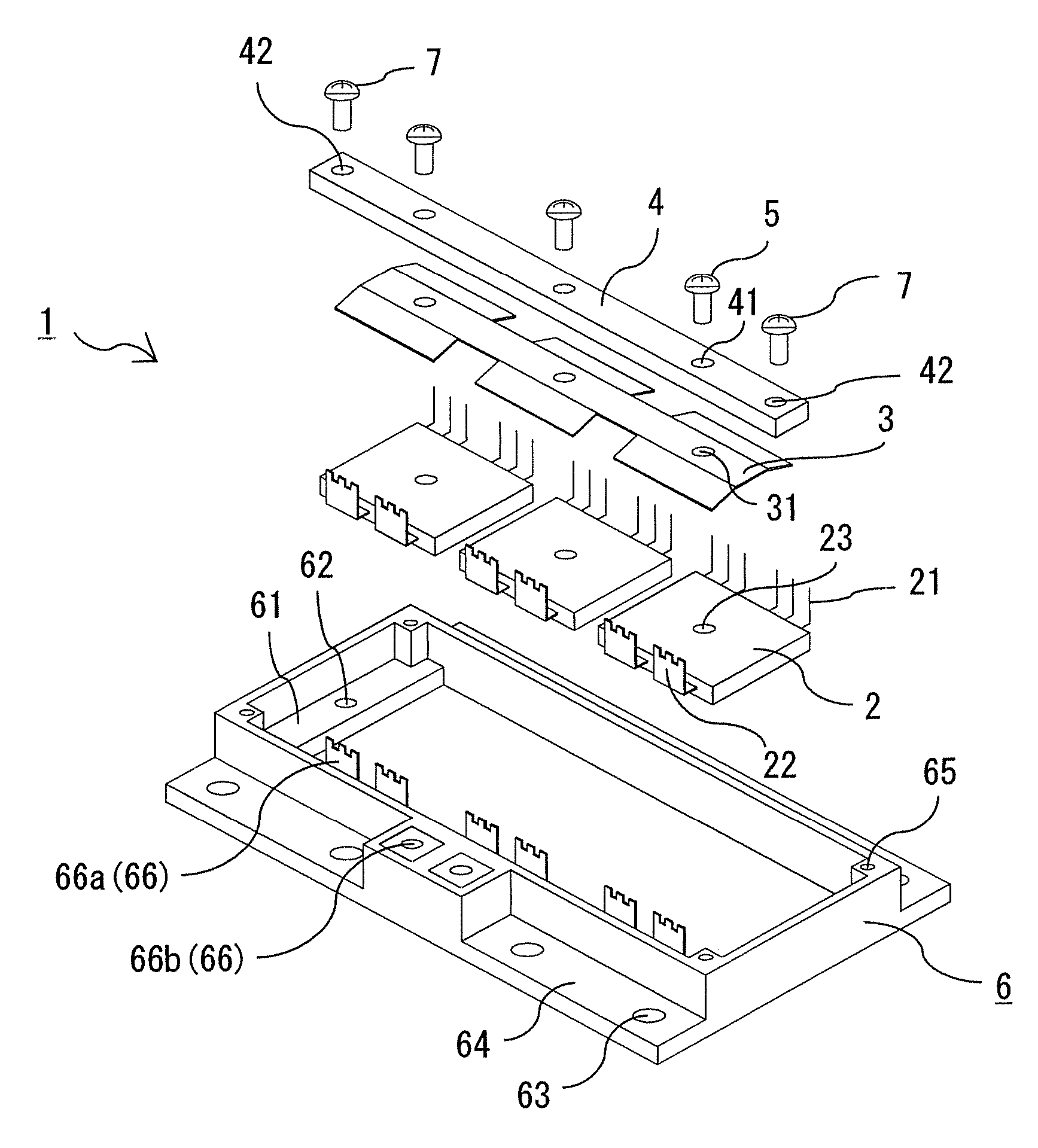
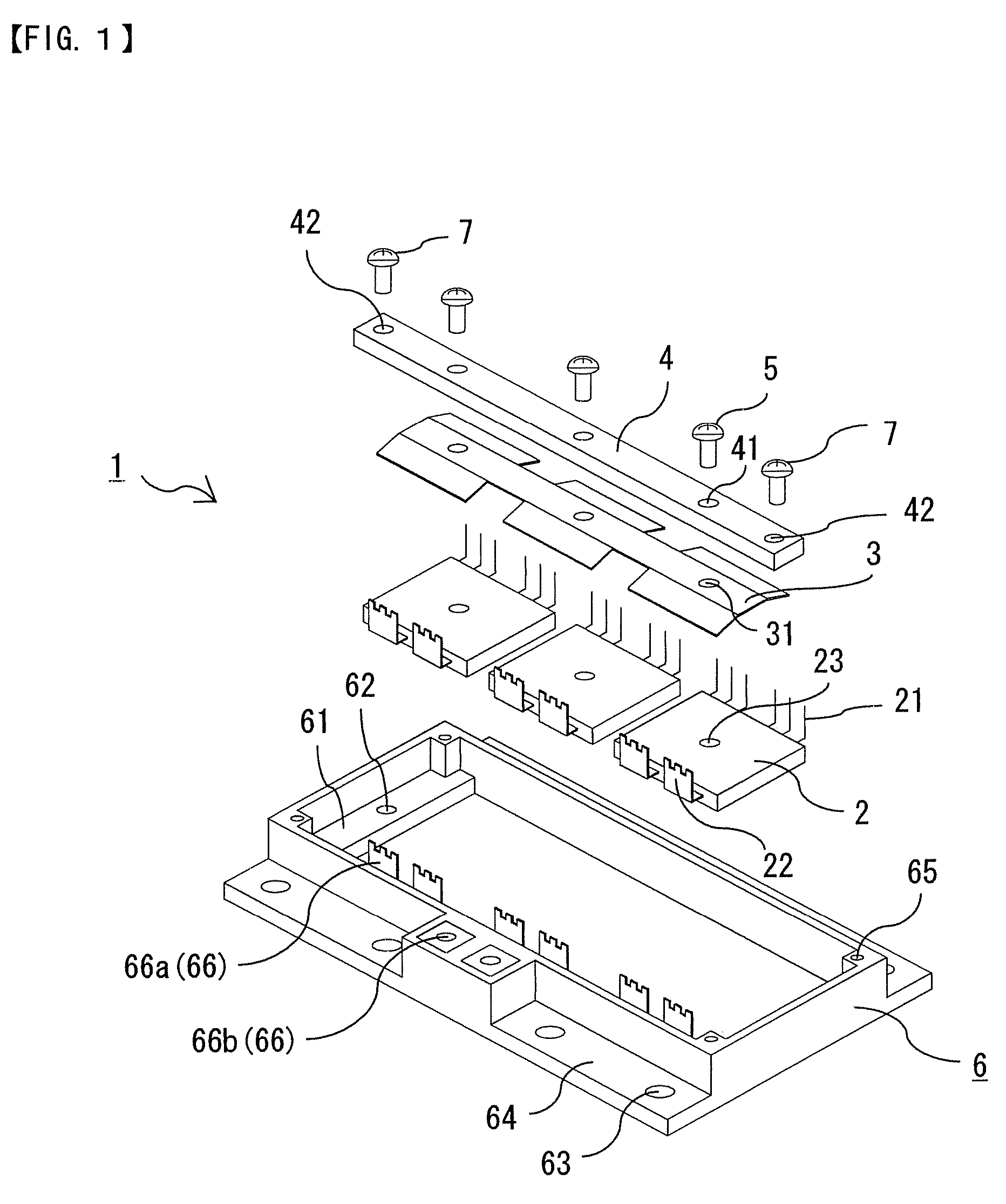
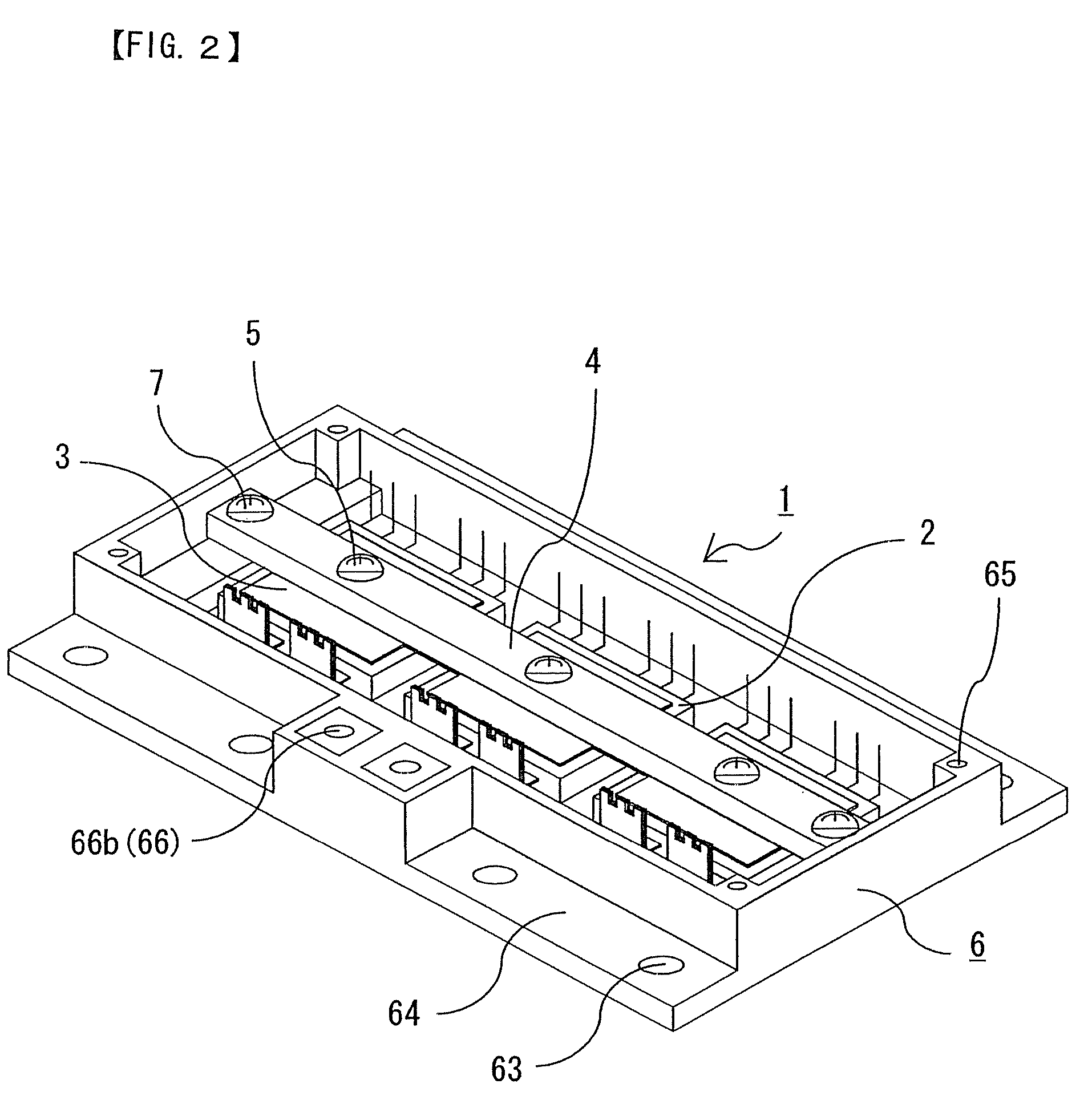
[0022]FIG. 1 is a broken perspective view showing a structure of a semiconductor device according to Embodiment 1 of this invention. FIG. 2 is a perspective view showing a state in which the semiconductor device of FIG. 1 is assembled. FIG. 3 is a sectional view showing a part of the semiconductor device of FIG. 2, wherein a frame part is omitted. FIG. 4 is a schematic diagram showing one example of fixing a cooling member and a control unit to the semiconductor device of FIG. 2.

[0023]Referring to FIGS. 1 to 3, a semiconductor device 1 is provided with semiconductor modules 2 in which semiconductor elements are sealed with a resin, a reinforcing beam 4 fixed to an upper surface of the semiconductor module 2 via a plate-like spring 3, a frame part 6 disposed in such a fashion as to enclose the semiconductor module 2, the plate-like spring 3, and the reinforcing beam 4, the reinforcing beam 4 having its both ends fixed to the frame part 6.

[0024]The semiconductor modules 2 are provided...

embodiment 2

[0048]While the frame part 6 is made from the synthetic resin material in Embodiment 1, the frame part is made from a metal having high rigidity in Embodiment 2. FIG. 5 is a broken perspective view showing a structure of a semiconductor device according to Embodiment 2 of this invention. FIG. 6 is a perspective view showing a state in which the semiconductor device of FIG. 5 is assembled. Components same as those of Embodiment 1 are denoted by the same reference numerals, and descriptions thereof are omitted.

[0049]Referring to FIGS. 5 and 6, a frame part 6 is made from a metal material having high rigidity, such as iron, aluminum, and magnesium, and produced by molding, die casting, or the like. Since the frame part 6 itself is formed from the electroconductive material, it is difficult to adapt the structure of Embodiment 1 wherein the bus bars serving as electroconductive parts are formed by insertion molding, and the connection terminal and the external terminal are exposed. Acco...

embodiment 3

[0053]While the frame part and the reinforcing beam are formed as separate components and fixed by the screw and the like in Embodiments 1 and 2, the frame part is integrally formed with the reinforcing beam in Embodiment 3. A material for the frame part may be the synthetic resin as in Embodiment 1 or the metal material as in Embodiment 2 depending on the object, and the case of using the metal material will be described in Embodiment 3.

[0054]FIG. 7 is a broken perspective view showing a structure of a semiconductor device according to Embodiment 3 of this invention. FIG. 8 is a perspective view showing a state in which the semiconductor device of FIG. 7 is assembled. Components same as those of Embodiment 1 are denoted by the same reference numerals, and descriptions thereof are omitted.

[0055]As shown in FIGS. 7 and 8, the semiconductor module 2 and a plate-like spring 300 fixed to the upper surface of the semiconductor module 2 are disposed below a beam part 601 formed integrally...


PUM


Abstract

The present invention is intended to obtain a semiconductor device that is reduced in size, weight, and cost and improved in performance stability and productivity.The semiconductor device includes a semiconductor module in which a semiconductor element is sealed with a resin, a reinforcing beam fixed to an upper surface of the semiconductor module via a plate-like spring, and a frame part to which both ends of the reinforcing beam are fixed, the frame part being disposed in such a fashion as to enclose from four directions an outer periphery of the semiconductor module, plate-like spring, and the reinforcing beam.

Description

BACKGROUND OF THE INVENTION[0001]1. Field of the Invention[0002]This invention relates to a semiconductor device provided with a semiconductor module that is mounted on a mobile object such as a vehicle, the invention contributing particularly to a reduction in influence of a thermal stress due to heating.[0003]2. Description of the Background Art[0004]Conventional semiconductor device is generally provided with a semiconductor module having a semiconductor element sealed with a resin and a screw through-hole provided at a central part thereof, a plate-like presser spring disposed at one side of the semiconductor module, a reinforcing beam for reinforcing the presser plate-like spring, and a heatsink disposed at the other side of the semiconductor module, wherein the semiconductor module is fixed to the heatsink by a screw inserted from the reinforcing beam side into the screw through-hole of the semiconductor module via the reinforcing beam and the presser plate-like spring, and th...

Claims


Application Information

Patent Timeline
Patent Type & Authority Patents(United States)
IPC IPC(8): H01L23/34
CPCH01L23/16H05K7/2049H01L2924/12044H01L2924/0002H01L2924/00H01L23/40H01L23/48
Inventor KIMURA, TORUSHIRAKATA, YUJI
Owner MITSUBISHI ELECTRIC CORP
Why Eureka
Try Eureka