Density gradient-free gap fill

a gradient-free, gap-free technology, applied in the direction of semiconductor/solid-state device manufacturing, basic electric elements, electric apparatus, etc., can solve the problems of void-free filling or uniform lining of high aspect ratio spaces (e.g., ar>6:1) becoming increasingly difficult, and forming cusps, also known as overhangs

Active Publication Date: 2011-02-15
NOVELLUS SYSTEMS
View PDF34 Cites 66 Cited by
  • Summary
  • Abstract
  • Description
  • Claims
  • Application Information

AI Technical Summary

Problems solved by technology

As device geometries shrink and thermal budgets are reduced, void-free filling or uniform lining of high aspect ratio spaces (e.g., AR>6:1) becomes increasingly difficult due to limitations of existing deposition processes.
Nevertheless, HDP CVD gapfill results in the formation of cusps, also known as overhangs, at the entry region of the gap to be filled.
As a result, the entry region of a high aspect ratio structure may close before bottom-up fill has been completed, leaving voids or weak spots within the structure.
This problem is exacerbated in small features.
However, these etch steps may be inappropriate in some applications.

Method used


Image

  • Density gradient-free gap fill
  • Density gradient-free gap fill
  • Density gradient-free gap fill

Examples


Embodiment Construction

Introduction

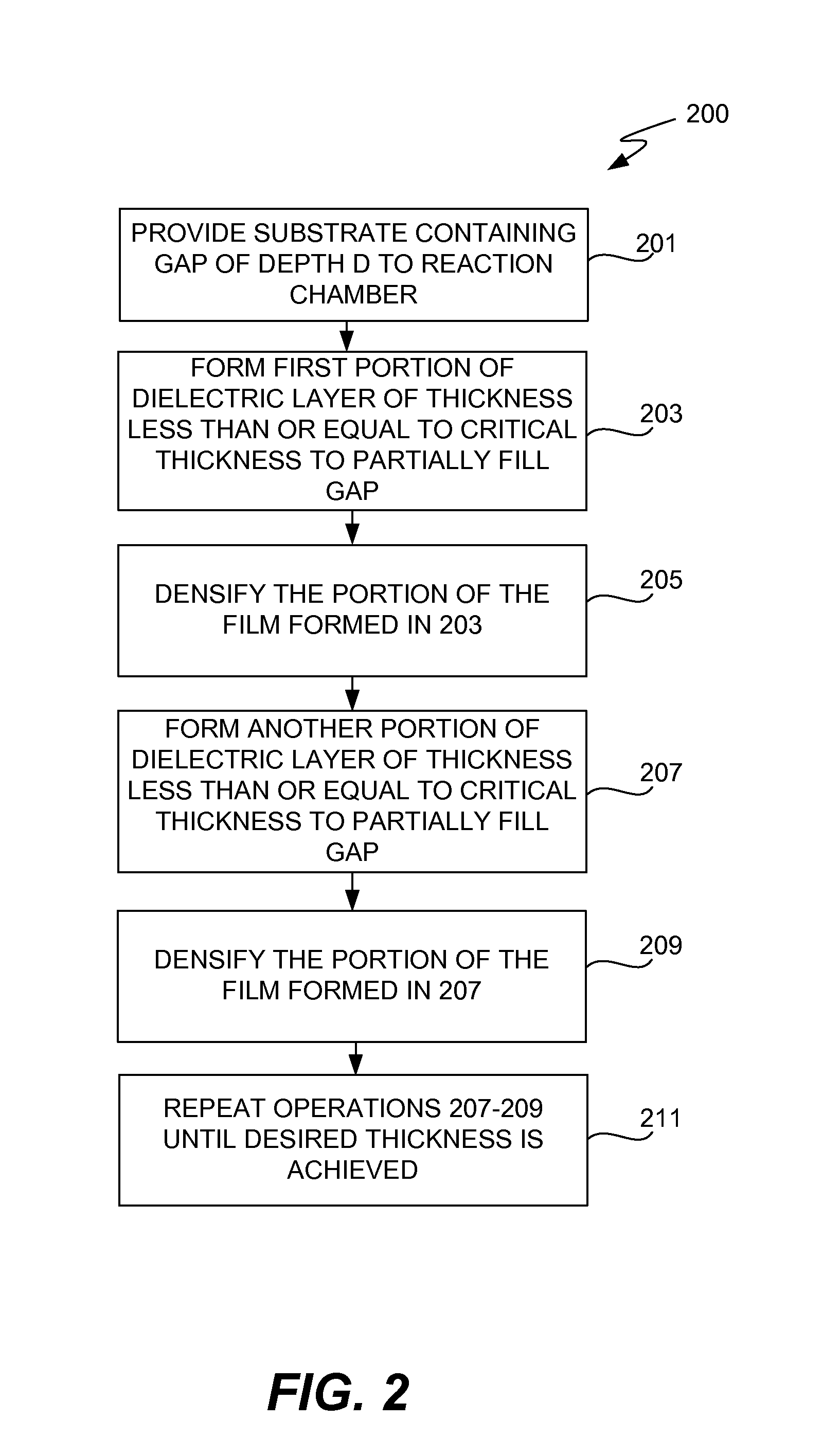
[0019]The present invention relates to deposition processes that provide dielectric gap fill of high aspect ratio (typically at least 6:1), narrow width (typically less than 0.13 um) gaps. The methods of the invention provide uniform, i.e. void-free and density gradient-free, gapfill.

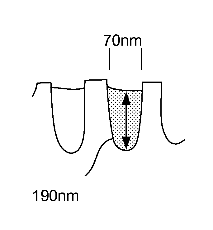
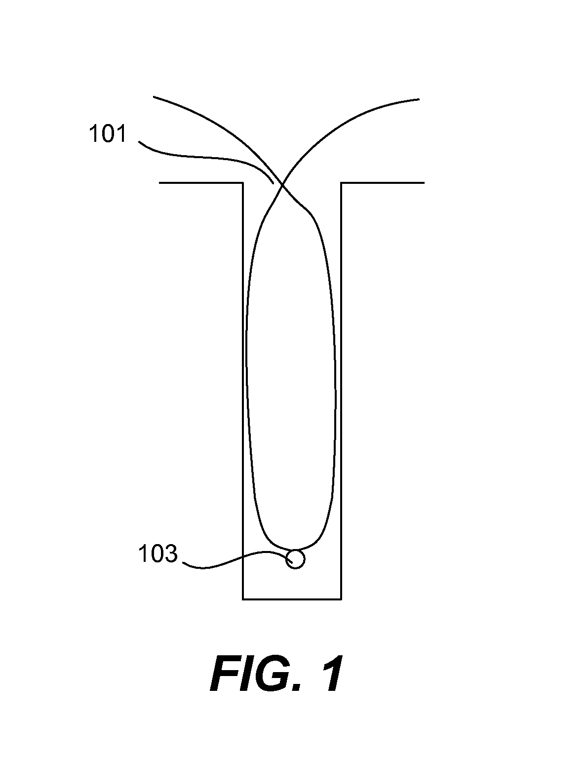
[0020]The methods are particularly useful at technology nodes of 65 nm and below, for which conventional methods of dielectric gapfill may have various shortcomings. For example, neither conventional high density plasma chemical vapor deposition (HPD-CVD) nor sub-atmospheric CVD (SACVD) methods do provide void-free gapfill of high aspect ratio structures, especially of structures having re-entrant profiles. Those methods either deposit more material on the upper region than on the lower region of a sidewall or form cusps (also called overhangs) at the entry of the gap. FIG. 1 shows a rough schematic of a trench partially filled by such a process. Reference number 101 indicates where sidewall...


PUM

PropertyMeasurementUnit
critical thicknessaaaaaaaaaa
widthaaaaaaaaaa

Abstract

Multi-cycle methods result in dense, seamless and void-free dielectric gap fill are provided. The methods involve forming liquid or flowable films that partially fill a gap, followed by a solidification and / or anneal process that uniformly densifies the just-formed film. The thickness of the layer formed is such that the subsequent anneal process creates a film that does not have a density gradient. The process is then repeated as necessary to wholly or partially fill or line the gap as desired. The methods of this invention may be used to line or fill high aspect ratio gaps, including gaps having aspect ratios greater than about 6:1 with widths less than about 0.13 μm.

Description

CROSS REFERENCE TO RELATED APPLICATIONS[0001]This application claims priority under 35 U.S.C. §119(e) to U.S. Provisional Application No. 60 / 856,193, filed Nov. 1, 2006, which is incorporated by reference herein and for all purposes.BACKGROUND OF THE INVENTION[0002]This invention relates to electronic device fabrication processes. More specifically, the invention relates to chemical vapor deposition processes for forming dielectric layers in high aspect ratio, narrow width recessed features.[0003]It is often necessary in semiconductor processing to fill or line high aspect ratio gaps with insulating material. This is the case for shallow trench isolation (STI) layers, inter-metal dielectric (IMD) layers, inter-layer dielectric (ILD) layers, passivation layers, etc. As device geometries shrink and thermal budgets are reduced, void-free filling or uniform lining of high aspect ratio spaces (e.g., AR>6:1) becomes increasingly difficult due to limitations of existing deposition proce...

Claims


Application Information

Patent Timeline
Patent Type & Authority Patents(United States)
IPC IPC(8): H01L21/31H01L21/469
CPCH01L21/76224
Inventor WANG, FENGLU, VICTOR Y.LU, BRIANYAU, WAI-FAN
Owner NOVELLUS SYSTEMS
Why Eureka
Try Eureka