Tantalum sputtering target

a sputtering target and sputtering technology, applied in the direction of diaphragms, metal-working apparatus, metallic material coating processes, etc., can solve the problems of deterioration of sputtering deposition quality and inferior uniformity of films, and achieve superior deposition properties, high deposition speed, and superior

Active Publication Date: 2011-02-22
JX NIPPON MINING & METALS CORP
View PDF20 Cites 12 Cited by
  • Summary
  • Abstract
  • Description
  • Claims
  • Application Information

AI Technical Summary

Benefits of technology

[0014]Thus, an object of the present invention is to obtain a tantalum sputtering target having superior deposition properties where the deposition speed is high, film evenness (uniformity) is superior, and generation of arcings or particles is reduced in comparison to a conventional tantalum target with an arrangement with a specific crystal orientation.
[0015]In order to overcome the foregoing problems, the present inventors discovered that a tantalum sputtering target having superior deposition properties in comparison to conventional tantalum targets can be obtained by improving and devising the target structure and randomizing the crystal orientation.
[0020]The present invention yields a superior effect in that it is able to provide a tantalum sputtering target having superior deposition properties where the deposition speed is high, film evenness (uniformity) is superior, generation of arcings or particles is reduced and the use efficiency of the target is favorable in comparison to a conventional tantalum target with a crystal orientation arranged on the target surface.

Problems solved by technology

When sputtering is performed with a tantalum target as described above, there are problems in that the evenness (uniformity) of the film will become inferior, the generation of arcings and particles will be promoted, and the quality of sputtering deposition will deteriorate.

Method used


Image

  • Tantalum sputtering target
  • Tantalum sputtering target

Examples


example 1

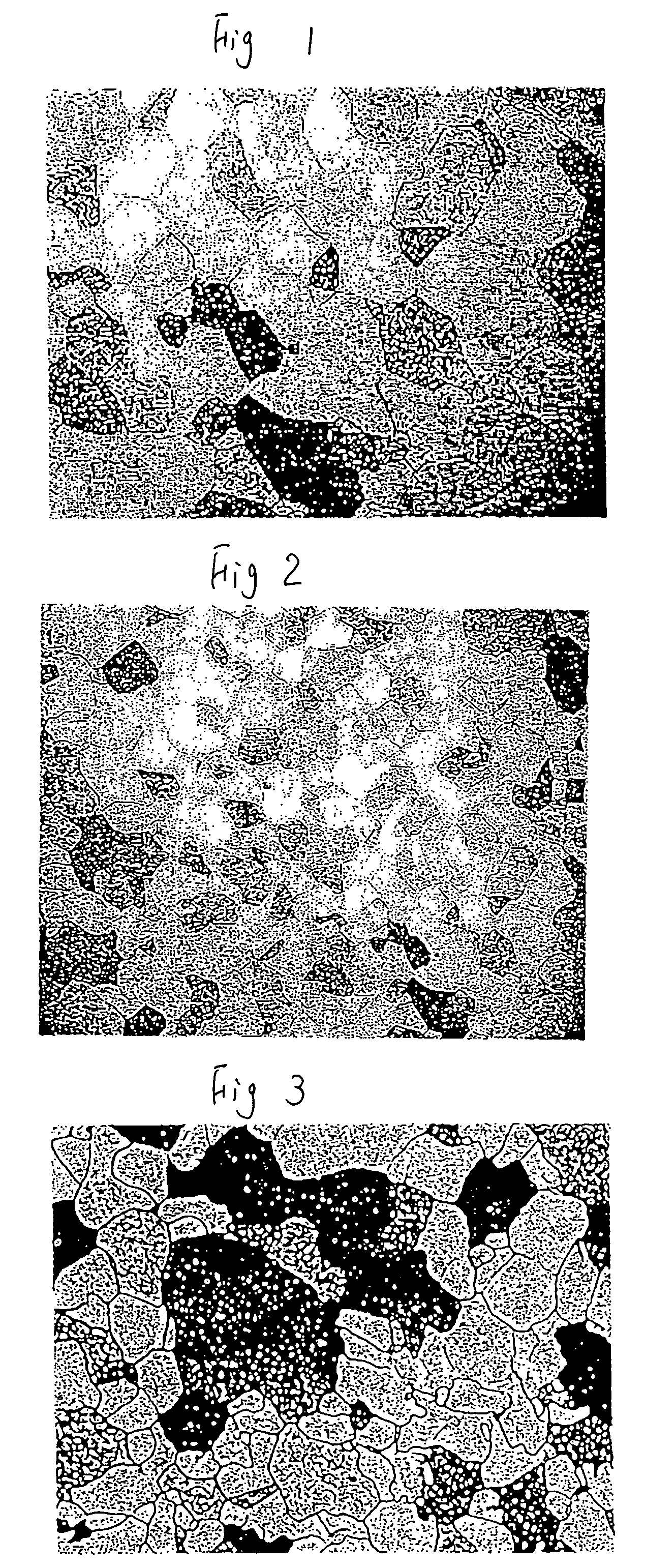
[0048]A tantalum raw material having a purity of 99.997% was subject to electron beam melting, and this was cast to prepare an ingot or billet having a thickness of 200 mm and diameter of 200 mm φ. The crystal grain diameter in this case was approximately 55 mm.

[0049]Next, after performing extend forging to this ingot or billet at room temperature, this was subject to recrystallization annealing at a temperature of 1500K. As a result, a material having a structure in which the average crystal grain diameter is 200 μm, thickness of 100 mm, and diameter of 100 mm φ was obtained.

[0050]Next, this was subject to extend forging and upset forging at room temperature once again, and recrystallization annealing was performed thereto again at a temperature of 1480K. As a result, a material having a structure in which the average crystal grain diameter is 100 μm, thickness of 100 mm, and diameter of 100 mm φ was obtained.

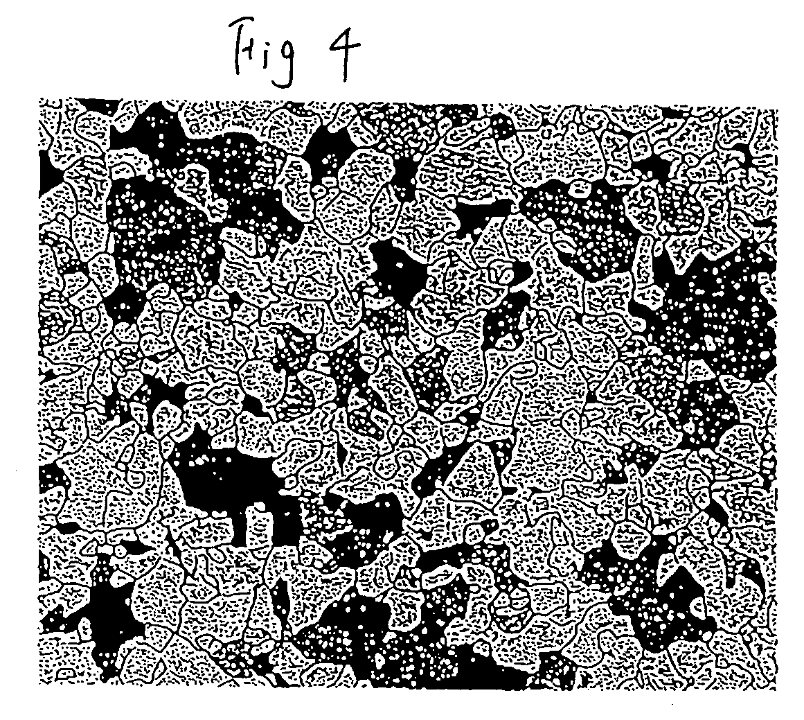
[0051]Next, this was subject to cold extend forging and upset forging, an...

example 2

[0059]A tantalum raw material having a purity of 99.997% was subject to electron beam melting, and this was cast to prepare an ingot or billet having a thickness of 200 mm and diameter of 200 mm φ. The crystal grain diameter in this case was approximately 50 mm.

[0060]Next, after performing extend forging to this ingot or billet at room temperature, this was subject to recrystallization annealing at a temperature of 1500K. As a result, a material having a structure in which the average crystal grain diameter is 200 μm, thickness of 100 mm, and diameter of 100 mm φ was obtained.

[0061]Next, this was subject to extend forging and upset forging at room temperature once again, and recrystallization annealing was performed thereto again at a temperature of 1173K. As a result, a material having a structure in which the average crystal grain diameter is 80 μm, thickness of 100 mm, and diameter of 100 mm φ was obtained.

[0062]Next, this was subject to cold extend forging and upset forging, and...

example 3

[0069]A tantalum raw material having a purity of 99.997% was subject to electron beam melting, and this was cast to prepare an ingot or billet having a thickness of 200 mm and diameter of 200 mm φ. The crystal grain diameter in this case was approximately 60 mm.

[0070]Next, after performing extend forging to this ingot or billet at room temperature, this was subject to recrystallization annealing at a temperature of 1500K. As a result, a material having a structure in which the average crystal grain diameter is 200 μm, thickness of 100 mm, and diameter of 100 mm φ was obtained.

[0071]Next, this was subject to extend forging and upset forging at room temperature once again, and recrystallization annealing was performed thereto again at a temperature of 1173K. As a result, a material having a structure in which the average crystal grain diameter is 80 μm, thickness of 100 mm, and diameter of 100 mm φ was obtained.

[0072]Next, this was subject to cold extend forging and upset forging, and...


PUM

PropertyMeasurementUnit
average crystal grain sizeaaaaaaaaaa
crystal grain diameteraaaaaaaaaa
crystal grain sizeaaaaaaaaaa

Abstract

A tantalum sputtering target, wherein when the sum of the overall crystalline orientation is 1 on a tantalum target surface, the area ratio of crystals having any orientation among (100), (111), (110) does not exceed 0.5. Thus, obtained is a tantalum sputtering target having superior deposition properties where the deposition speed is high, film evenness (uniformity) is superior, and generation of arcings or particles is reduced.

Description

BACKGROUND OF THE INVENTION[0001]The present invention relates to a tantalum sputtering target having a random crystalline orientation, high deposition speed, superior film evenness (uniformity), reduced generation of arcings or particles and favorable target use efficiency.[0002]In recent years, the sputtering method for forming a film from materials such as metal or ceramics has been used in numerous fields such as electronics, corrosion resistant materials and ornaments, catalysts, as well as in the manufacture of cutting / grinding materials and abrasion resistant materials.[0003]Although the sputtering method itself is a well-known method in the foregoing fields, recently, particularly in the electronics field, a tantalum sputtering target suitable for forming films of complex shapes and forming circuits is in demand.[0004]Generally, this tantalum target is manufactured by forging and annealing (heat treatment) an ingot or billet formed by performing electron beam melting and cas...

Claims


Application Information

Patent Timeline
Patent Type & Authority Patents(United States)
IPC IPC(8): C22C27/02C23C14/00C23C14/34
CPCC23C14/3414C23C14/34C23C14/02B21J1/02B21J5/00C22F1/18H01L21/02631
Inventor ODA, KUNIHIRO
Owner JX NIPPON MINING & METALS CORP
Why Eureka
Try Eureka