Semiconductor light detecting element including first and second multilayer light reflective structures sandwiching and contacting a light absorptive layer

a technology of semiconductors and light reflecting structures, applied in semiconductor devices, solid-state devices, radiation controlled devices, etc., can solve the problems of significant change in current output from pd and low wavelength stability, and achieve the effect of improving wavelength stability, affecting the and high wavelength dependence of quantum efficiency

Active Publication Date: 2011-02-22
MITSUBISHI ELECTRIC CORP
View PDF13 Cites 3 Cited by
  • Summary
  • Abstract
  • Description
  • Claims
  • Application Information

AI Technical Summary

Benefits of technology

[0009]Therefore, the present inventors analyzed why the wavelength dependence of the quantum efficiency was high in the PDs shown in FIGS. 9 and 10. In the PD shown in FIG. 9, a part of light incident into the absorptive layer 104 transmits in the n-type multilayer reflective layer 102 and enters into the n-type InP substrate 101. Then, the light that has entered in the n-type InP substrate 101 reciprocates between the cathode 108 and the n-type multilayer reflective layer 102, and generates a resonance mode in the n-type InP substrate 101. On the other hand, in the vicinity of the absorptive layer 104, the mode between the n-type multilayer reflective layer 102 and the p-type multilayer reflective layer 106, the mode between the n-type multilayer reflective layer 102 and the absorptive layer 104, and the mode between the p-type multilayer reflective layer 106 and the absorptive layer 104 are present. The present inventors clarified by calculations that since the three resonance modes in the vicinity of the absorptive layer 104 interfered with the resonance mode in the n-type InP substrate 101 to generate a composite resonance mode, the above-described wavelength dependence of quantum efficiency was generated. It was especially found that the resonance mode generated in the n-type phase adjusting layer 103 in the side close to the n-type InP substrate 101 joins with the resonance mode in the n-type InP substrate 101 to easily form a composite resonance mode, and strongly affects the wavelength dependence of quantum efficiency.
[0010]To solve the above-described problems, it is an object of the present invention to provide a semiconductor light receiving element that can improve wavelength stability.
[0012]According to the present invention, wavelength stability can be improved.

Problems solved by technology

Therefore, even if the wavelength of incident light was changed only by as small as 1 nm, a current outputted from the PD was significantly changed, and wavelength stability was low.

Method used


Image

  • Semiconductor light detecting element including first and second multilayer light reflective structures sandwiching and contacting a light absorptive layer
  • Semiconductor light detecting element including first and second multilayer light reflective structures sandwiching and contacting a light absorptive layer
  • Semiconductor light detecting element including first and second multilayer light reflective structures sandwiching and contacting a light absorptive layer

Examples


first embodiment

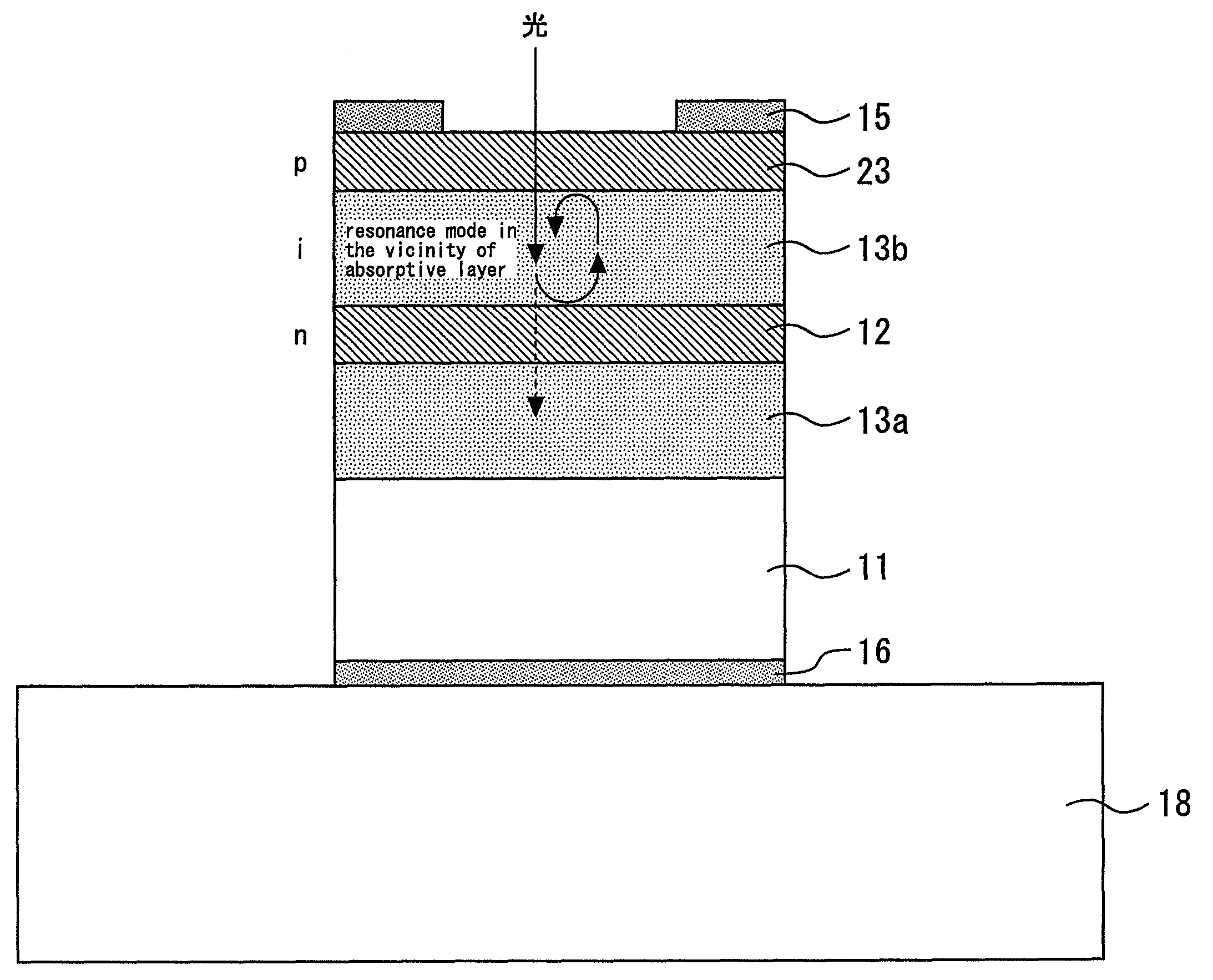
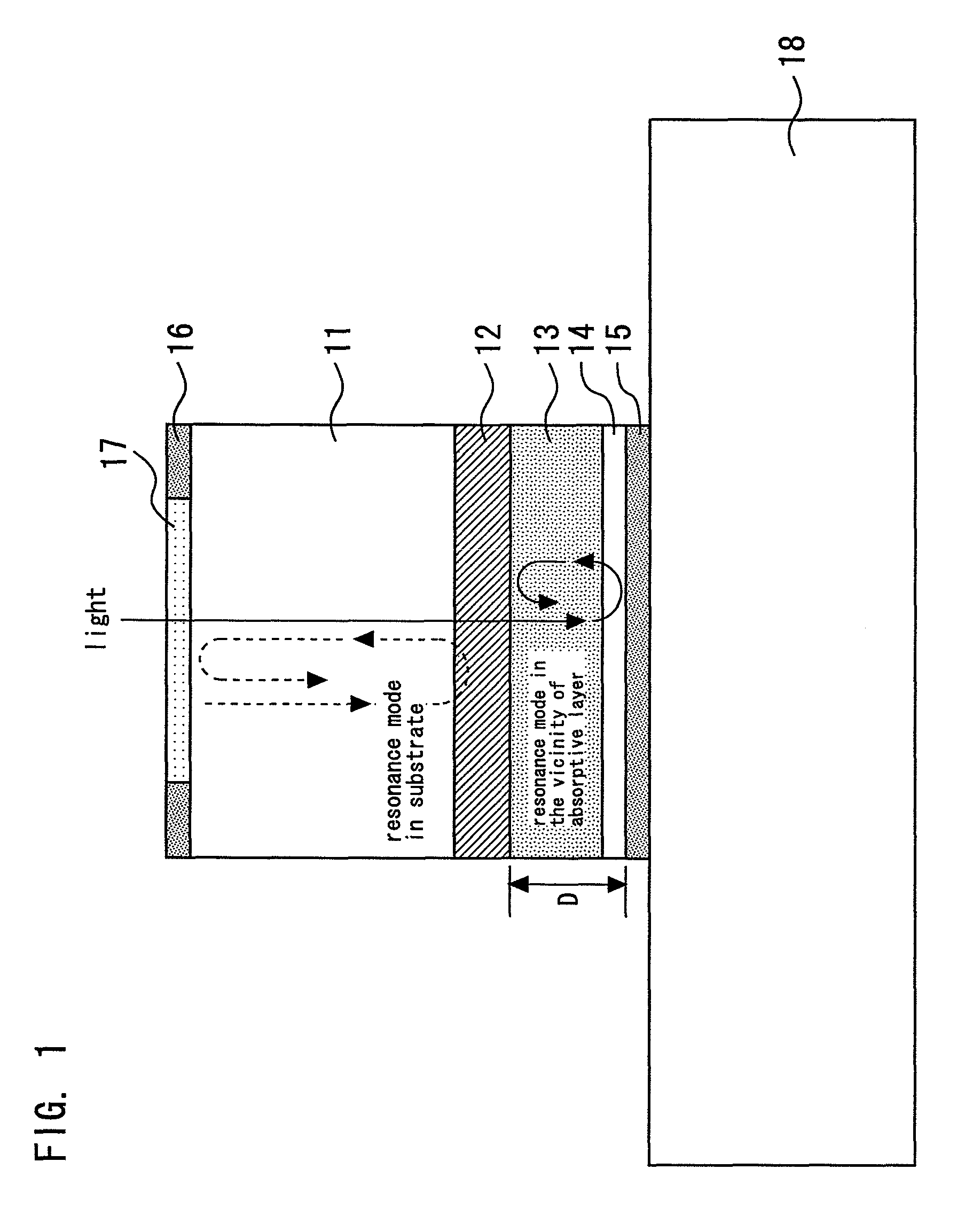
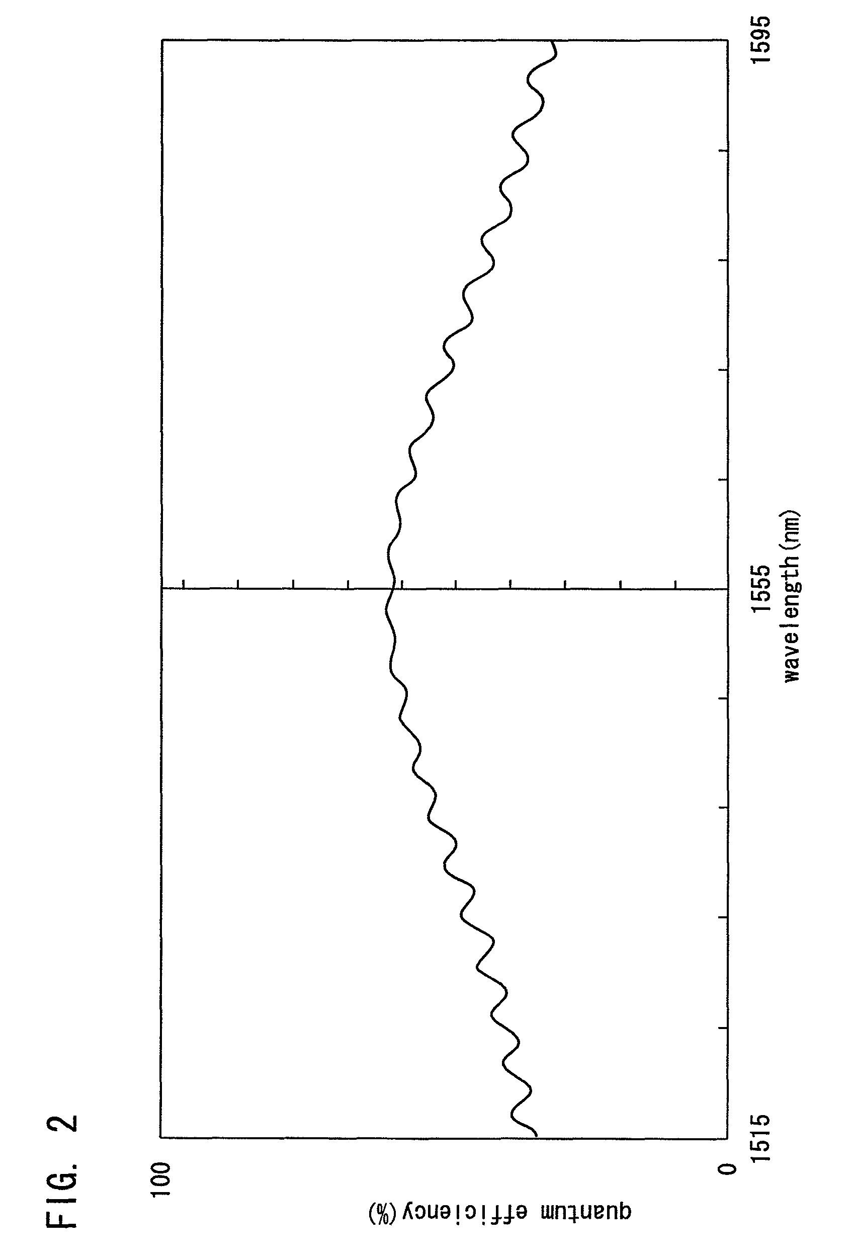
[0026]FIG. 1 is a sectional view showing a semiconductor light receiving element according to the first embodiment of the present invention. The semiconductor light receiving element according to the present embodiment is a backside incidence resonance photodiode (PD) receiving light radiated from the upper side of the drawing.

[0027]An n-type InP substrate 11 (semiconductor substrate) has a lower surface (first major surface) and an upper surface (second major surface) opposite to each other. An n-type multilayer reflective layer 12 (first reflective layer), an absorptive layer 13, a p-type phase adjusting layer 14 (phase adjusting layer), and an anode 15 (second reflective layer) are formed sequentially on the lower surface of the n-type InP substrate 11 from the side of the n-type InP substrate 11. A cathode 16 is formed on the upper surface of the n-type InP substrate 11. The cathode 16 has an opening for receiving light. An anti-reflection film 17 is formed in the opening of the...

second embodiment

[0042]FIG. 4 is a sectional view showing a semiconductor light receiving element according to the second embodiment of the present invention. A ring-shaped contact layer 21 is disposed on the peripheral portion of an anode 15 (second reflective layer) disposed in a light-receiving region, and is connected to a p-type phase adjusting layer 14. As the contact layer 21, a semiconductor layer having a smaller band gap than a band gap of the p-type phase adjusting layer 14, such as InGaAs and InGaAsP layers, or a metal having low contact resistance, such as AuZn, is used. Other configurations are identical to the configuration of the first embodiment.

[0043]Since the contact resistance of the anode 15 and the p-type phase adjusting layer 14 is lowered by the contact layer 21, heat generation is suppressed, and quantum efficiency is stabilized. The contact layer 21 may be provided on the entire surface between the p-type phase adjusting layer 14 and the anode 15. However, since the contact...

third embodiment

[0044]FIG. 5 is a sectional view showing a semiconductor light receiving element according to the third embodiment of the present invention. A reflection enhancing layer 22 (second reflective layer) having a high reflectivity is provided in the light-receiving region receiving light on a p-type phase adjusting layer 14. A ring-shaped contact layer 21 is disposed on the peripheral portion of the reflection enhancing layer 22, and is connected to the p-type phase adjusting layer 14. An anode 15 (metal film) is provided on the reflection enhancing layer 22 and the contact layer 21. Other configurations are identical to the configuration of the first embodiment.

[0045]By providing the reflection enhancing layer 22, the quantum efficiency of the PD can be further elevated. As the reflection enhancing layer 22, a single-layer or multilayer film of a dielectric material, such as Si3N4, SiO2, amorphous Si, Al2O3, and TiO2 can be used. In this case, since the alloying of the p-type phase adju...


PUM


Abstract

A semiconductor light detecting element comprises: a semiconductor substrate having a first major surface and a second major surface opposite each other; a first reflective layer, an absorptive layer, a phase adjusting layer, and a second reflective layer sequentially disposed, from the semiconductor substrate, on the first major surface of the semiconductor substrate; and an anti-reflection film on the second major surface of the semiconductor substrate. The first reflective layer is a multilayer reflective layer including laminated semiconductor layers having different refractive indices; the absorptive layer has a band gap energy smaller than band gap energy of the semiconductor substrate; the phase adjusting layer has a band gap energy larger than the band gap energy of the absorptive layer; and the first reflective layer contacts the absorptive layer, without intervention of other layers.

Description

BACKGROUND OF THE INVENTION[0001]1. Field of the Invention[0002]The present invention relates to a semiconductor light receiving element that can improve wavelength stability.[0003]2. Background Art[0004]FIG. 9 is a sectional view showing a surface incidence resonance photodiode (PD). An n-type multilayer reflective layer 102, an n-type phase adjusting layer 103, an i-type InGaAs absorptive layer 104, a p-type phase adjusting layer 105, and a p-type multilayer reflective layer 106 are sequentially formed on an upper surface of an n-type InP substrate 101. An anode 107 is formed on the p-type multilayer reflective layer 106, and a cathode 108 is formed on a lower surface of the n-type InP substrate 101. The PD is mounted on a pedestal 109.[0005]The n-type multilayer reflective layer 102 and the p-type multilayer reflective layer 106 are layers formed by laminating semiconductor layers having different refractive indices, for example, InP and InGaAsP, and have a function to reflect or...

Claims


Application Information

Patent Timeline
Patent Type & Authority Patents(United States)
IPC IPC(8): H01L31/0216
CPCB82Y20/00H01L31/02327H01L31/105H01L31/035236
Inventor ISHIMURA, EITARONAKAJI, MASAHARU
Owner MITSUBISHI ELECTRIC CORP
Why Eureka
Try Eureka