Silicon carbide semiconductor device having junction barrier Schottky diode

a silicon carbide semiconductor and junction barrier technology, applied in the direction of semiconductor devices, basic electric elements, electrical appliances, etc., can solve problems such as failure of semiconductor devices, and achieve the effect of higher break down voltag

Inactive Publication Date: 2011-02-22
DENSO CORP
View PDF14 Cites 21 Cited by
  • Summary
  • Abstract
  • Description
  • Claims
  • Application Information

AI Technical Summary

Benefits of technology

[0008]According to the above silicon carbide semiconductor device, since the radial width of the another one of the plurality of second conductivity type layers is larger than that of the one of the plurality of second conductivity type layers, an electric field is harder to concentrate at a boundary area between the Schottky electrode and the drift layer. It is possible to provide the silicon carbide semiconductor device with a higher break down voltage.

Problems solved by technology

Such electric concentration may cause failure of the semiconductor device.

Method used


Image

  • Silicon carbide semiconductor device having junction barrier Schottky diode
  • Silicon carbide semiconductor device having junction barrier Schottky diode
  • Silicon carbide semiconductor device having junction barrier Schottky diode

Examples


first embodiment

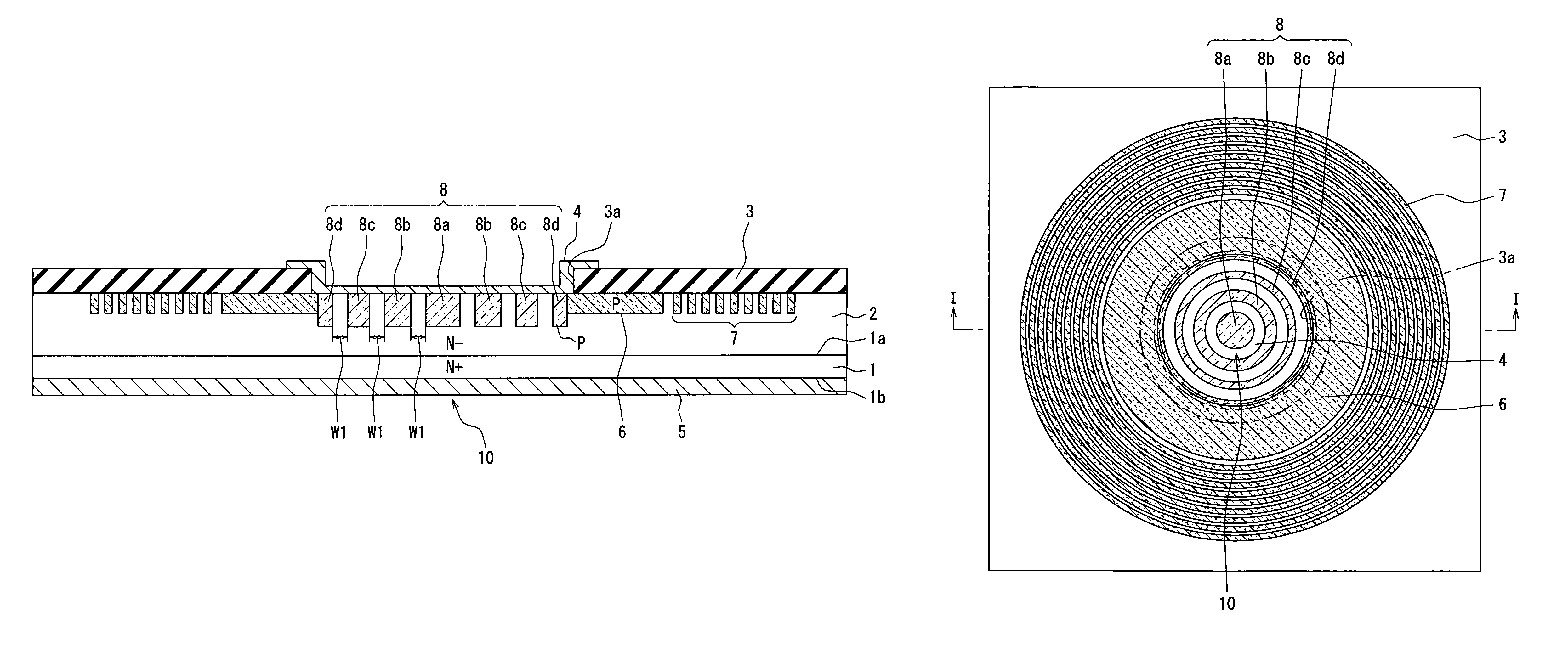
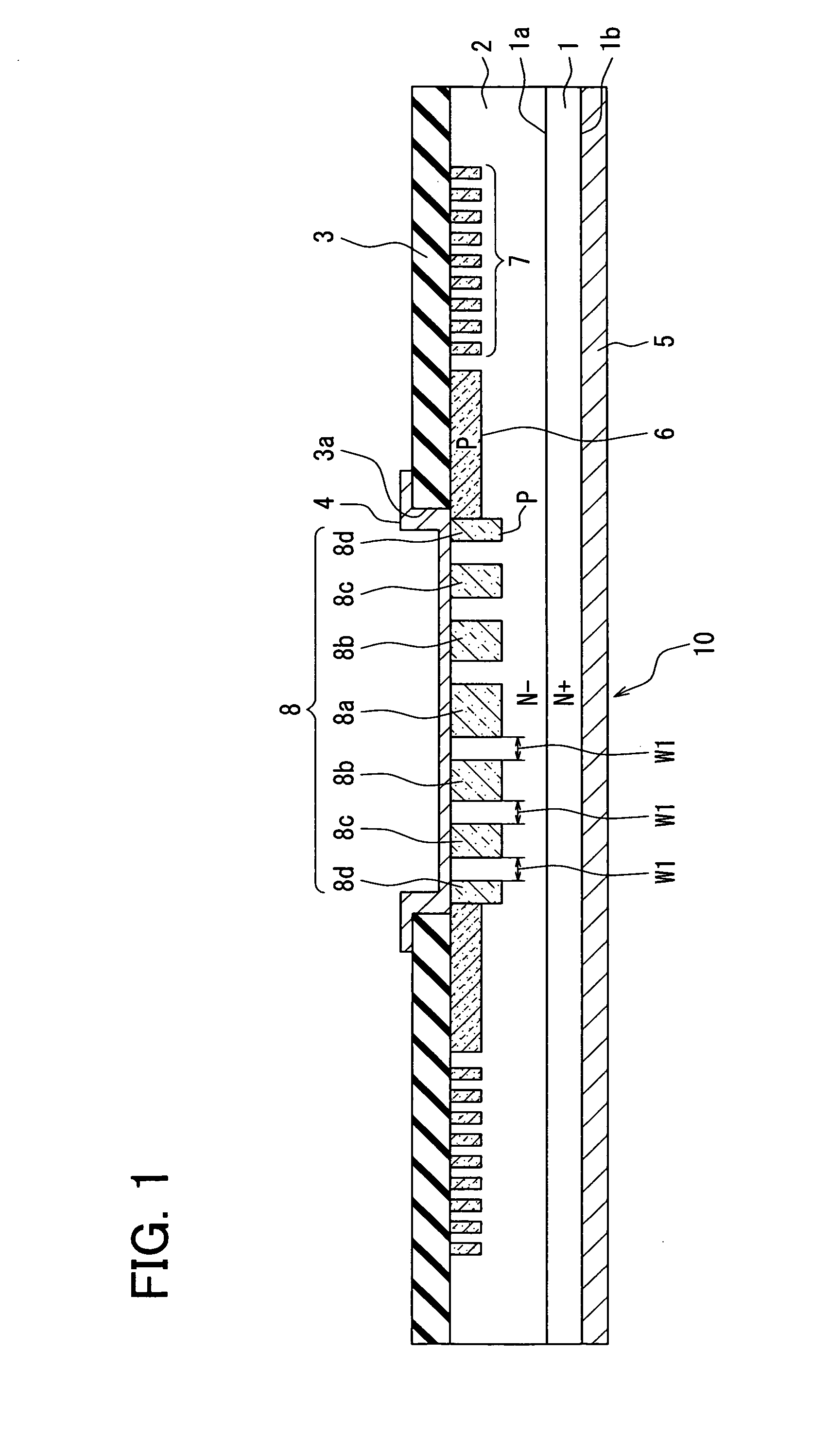
[0020]An SiC semiconductor device having a JBS according to a first embodiment is described below with reference to FIGS. 1 and 2.

[0021]The SiC semiconductor device includes an N+ type substrate 1 made of SiC, the N− type drift layer 2 made of SiC. An impurity concentration of the N+ type substrate 1 is in a range, for example, between 2×1018 cm−3 and 1×1021 cm−3. The N+ type substrate 1 includes a top surface 1a and a bottom surface 1b opposite to each other. The top surface 1a and the bottom surface 1b are also referred to hereinafter as a principal surface 1a and a rear surface 1b, respectively. The N− type drift layer 2 made of SiC is disposed on the principal surface 1a. The N− type drift layer 2 may be a stacked layer. A dopant concentration of the N− type drift layer 2 is, for example, in a range between 2.5×1015 cm−3 and 7.5×1015 cm−3 and lower than that of the N+ type substrate 1. A portion of the N+ type substrate 1 and a portion of the N− type drift layer 2 provide a cell...

second embodiment

[0039]An SiC semiconductor device having a JBS according to a second embodiment is described below with reference to FIG. 4. Geometry of P type layers 8 according to the present embodiment is different from that of the P type layers 8 according to the first embodiment.

[0040]As shown in FIG. 4, a depth of each P type layer 8 is deeper than that of the P type resurf layer 6 and the P type guard ring layers 7 in a direction, for example, substantially perpendicular to the principal surface 1a of the substrate 1. The P type resurf layer 6 and the P type guard ring layers 7 are included in the termination structure. The depth of each P type layer 8 is, for example, in a range between 0.7 μm and 1.5 μm. A depth difference between each P type layer 8 and the P type resurf layer 6 is in a range between 0.2 μm and 1.0 μm. A depth difference between each P type layer 8 and each P guard ring layer 7 is also in the range between 0.2 μm and 1.0 μm.

[0041]Since each P type layer 8 is deeper than t...

third embodiment

[0042]An SiC semiconductor device having a JBS according to a third embodiment is described below with reference to FIG. 6. Depths of P type layers 8 according to the present embodiment are different from that of the P type layers 8 according to the first and second embodiments.

[0043]As shown in FIG. 6, a depth of one of the multiple P type layers is less than or equal to that of another one of the multiple P type layers, wherein the another one is disposed adjacent to the one of the multiple P type layers 8 and disposed closer to the center of the contact region than the one of the multiple P type layers 8. Some of the P type layers located around the center member 8a are configured to have a substantially equal depth. According to the above structure, when a depletion layer is created below a central portion of the contact region between the Schottky electrode 4 and the N− type drift layer 2, the depletion layer is located in a deep portion of the N− type drift layer 2. An electri...


PUM


Abstract

A silicon carbide semiconductor device includes a substrate; a drift layer having a first conductivity type; an insulating layer; a Schottky electrode; an ohmic electrode; a resurf layer; and second conductivity type layers. The drift layer and the second conductivity type layers provide multiple PN diodes. Each second conductivity type layer has a radial width with respect to a center of a contact region between the Schottky electrode and the drift layer. A radial width of one of the second conductivity type layers is smaller than that of another one of the second conductivity type layers, which is disposed closer to the center of the contact region than the one of the second conductivity type layers.

Description

CROSS REFERENCE TO RELATED APPLICATION[0001]The present application is based on Japanese Patent Application No. 2007-143328 filed on May 30, 2007, the disclosure of which is incorporated herein by reference.FIELD OF THE INVENTION[0002]The present invention relates to a silicon carbide semiconductor device having a junction barrier Schottky diode (JBS).BACKGROUND OF THE INVENTION[0003]In a Schottky barrier diode (SBD), at an interface between a Schottky electrode made of metal and a semiconductor region, a work function difference between the metal and semiconductor is typically small. Because of the material property difference, a leakage current of the SBD may be relatively larger than that of a PN diode when the diodes are reverse-biased.[0004]Japanese Unexamined Patent Application Publication Number 2000-294804 shows a semiconductor device having a JBS, in which a PN diode is disposed on a part of a Schottky junction to suppress a leakage current when reverse-biased. The semicond...

Claims


Application Information

Patent Timeline
Patent Type & Authority Patents(United States)
IPC IPC(8): H01L29/66
CPCH01L29/0619H01L29/063H01L29/0692H01L29/1608H01L29/872
Inventor YAMAMOTO, TAKEOOKUNO, EIICHI
Owner DENSO CORP
Why Eureka
Try Eureka