Digital and analog IM3 product compensation circuits for an RF receiver

a technology of product compensation circuit and receiver, which is applied in the field of digital and analog im3 product compensation circuits of rf receivers, can solve the problems of infeasibility, inability to use one or more expensive off-chip filters, and the signal center frequency is quite high in the first few stages of the rf receiver to remove the signals from the unwanted frequency range. , to achieve the effect of reducing the cost of off-chip filters

Inactive Publication Date: 2011-02-22
CALIFORNIA INST OF TECH
View PDF16 Cites 16 Cited by
  • Summary
  • Abstract
  • Description
  • Claims
  • Application Information

AI Technical Summary

Problems solved by technology

Thus, completely removing the signals from the unwanted frequency range in the first few stages of the RF receiver, where the signal center frequency is quite high, is infeasible.
Typically, one or more expensive off-chip filters are used to partially attenuate the undesired frequency bands within the first few blocks of the RF receiver.
These signals in the unwanted frequency range typically interact with nonlinearities within the RF circuitry and may produce undesirable signal products within the desired signal band.
If either the costly filters mentioned above were removed to reduce component count or the block nonlinearities were reduced in order to save power or area, the undesirable signal products can have the effect of disabling the operation of the complete RF receiver system.
The use of a resistor for degeneration purposes, however, increases the noise contributed by the block.
Typically the desired signal amplitude is small and any additional noise contributions can easily bury the desired signal.
This issue can be avoided by degenerating the transconductance amplifier with an inductor; however, this solution requires a large amount of area and is frequency-selective, that is, it would be unsuitable for emerging wideband communication systems such as orthogonal frequency-division multiplexing (OFDM).
Furthermore, the level of improvement obtained is limited and has the effect of reducing the gain and other desirable properties of the amplifier.
This paper brings up the point that in order to completely cancel IM3 products in a typical single-ended BJT common-emitter amplifier, unacceptable conditions must be imposed on the input and output loading on the amplifier from a noise and power match perspective.
In general, bias-point specific compensation techniques such as these are sensitive to process, supply voltage, and temperature when implemented monolithically on a silicon die.
Also, measurements of the actual circuit reported in this paper show a 30 dB reduction in peak IIP3 from the idealized circuit in simulation, suggesting that the cancellation technique is not robust in practice.
Furthermore, the differential nature of this amplifier is problematic in that it requires two on-chip center-tapped transformers for a monolithic implementation.
In practice, this technique is area-intensive and would seldom be incorporated in a commercial integrated circuit.
However, because this technique depends on the gate biasing of the circuit, the beneficial effects of this technique will break down for large input voltage swings, which is especially a problem at the mixer.
This reduces the compression point (ICP1) of the circuit and hence increases its susceptibility to desensing by extremely large signals.
However, the LMS algorithm does not in this case compensate for delay through the duplexer and its performance is thus limited over chip-to-chip variation to less than what is required to remove the off-chip filter prior to the mixer.

Method used


Image

  • Digital and analog IM3 product compensation circuits for an RF receiver
  • Digital and analog IM3 product compensation circuits for an RF receiver
  • Digital and analog IM3 product compensation circuits for an RF receiver

Examples


Embodiment Construction

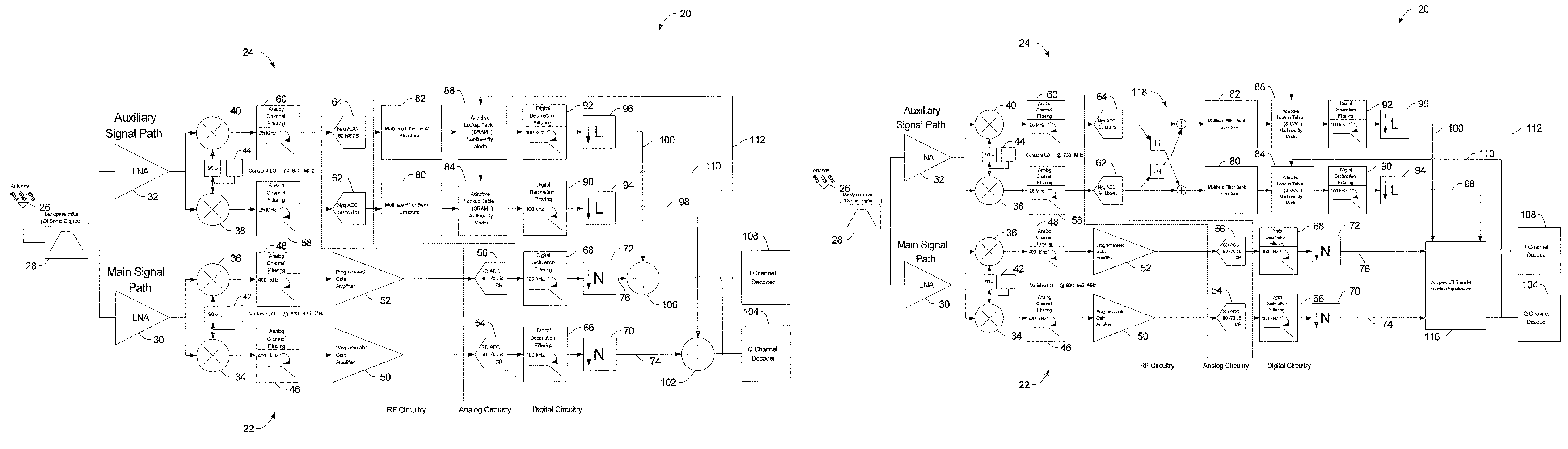
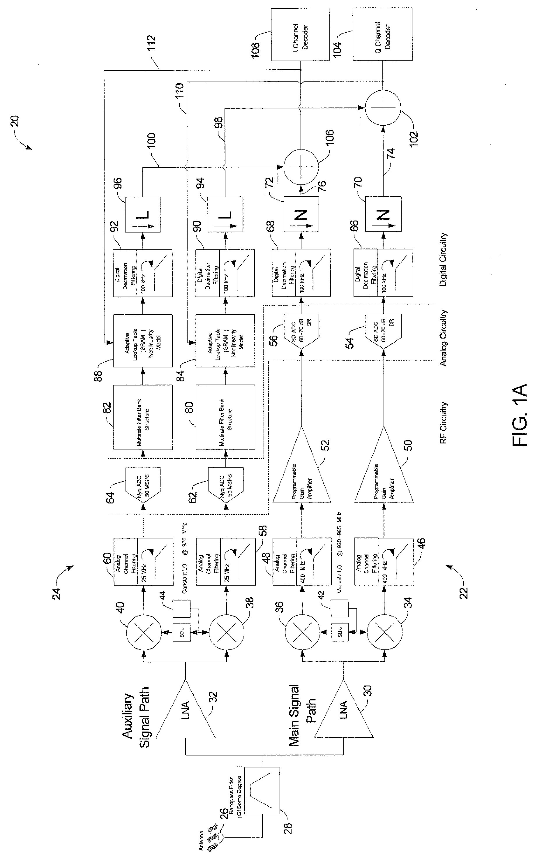
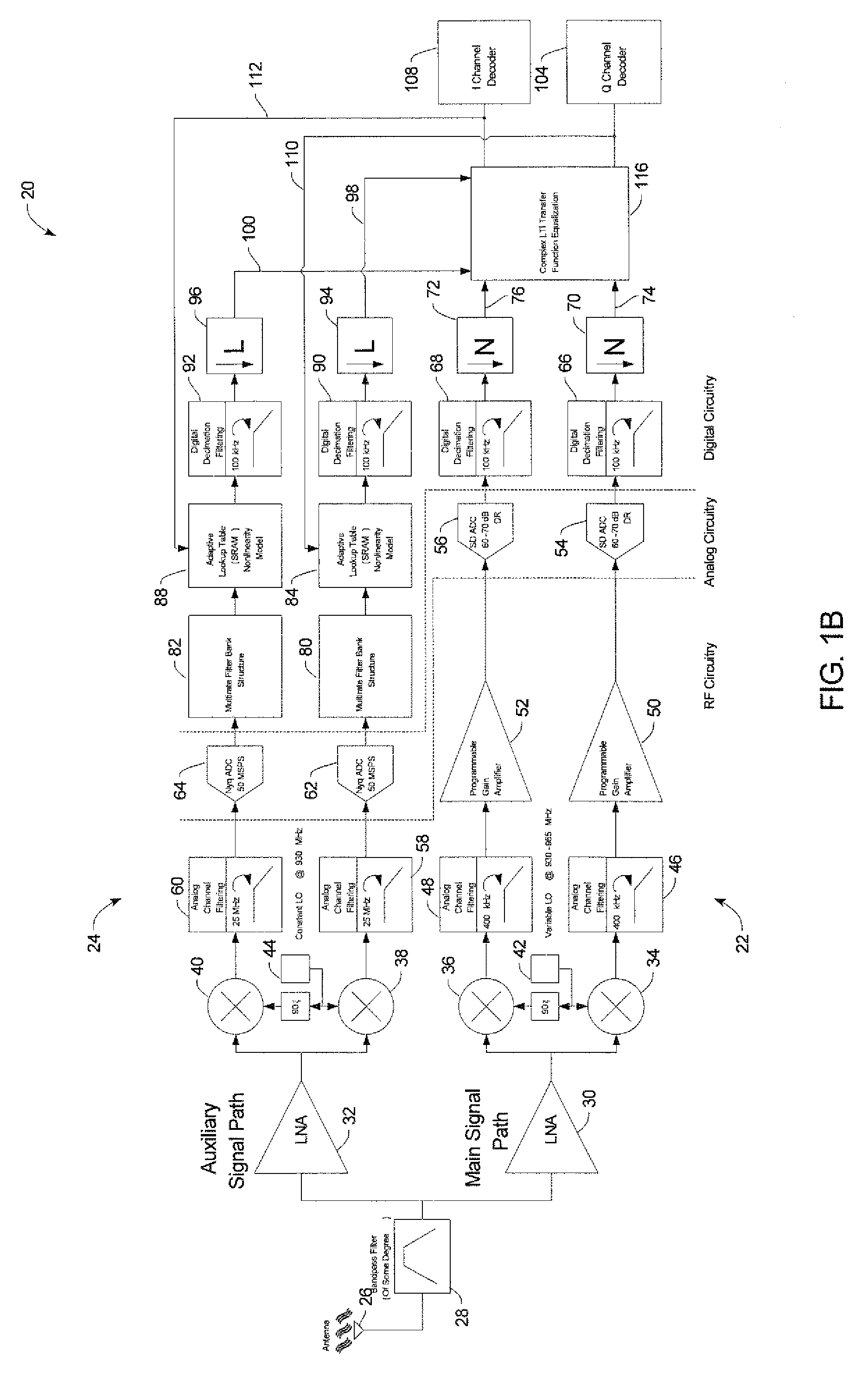
[0058]FIG. 1A is a schematic diagram 20 of one embodiment of al RF receiver with attenuated generated IM3 products according to the present invention which has a typical main signal path 22 driven by a low noise amplifier 30 and an auxiliary signal path 24 driven by another low noise amplifier 32. Both of the signal paths 22, 24 receive an RF signal from an antenna 26 which is passed through a bandpass filter 28 to the low noise amplifiers 30, 32. In another embodiment a single LNA could be used for both signal paths. Each of the signal paths 22, 24 has two mixers 34, 36 and 38, 40, respectively, for shifting the RF signal to baseband and separating the I and Q channels, respectively, of the RF signal. The main signal path 22 has a variable local oscillator (LO) 42 which in one embodiment may operate in the frequency range of 935-960 MHz, the frequency range used in GSM cell phones, while the auxiliary signal path 24 may have a LO with a constant frequency of 935 MHz in this embodim...


PUM


Abstract

Third-order intermodulation products (IM3) are attenuated in RF receivers by providing a typical main signal path and a parallel auxiliary signal path in which the IM3 products are accentuated, and the output from the main signal path is adaptively filtered to attenuate the IM3 products. In one embodiment, a multirate filter bank (MRFB) with asymmetric analysis and synthesis sections is used to detect and isolate the IM3 products. In another embodiment an analog nonlinear term generator is placed at the front of the auxiliary signal path. The analog nonlinear term generator takes advantage of the nonlinearities of a differential MOSFET circuit and a multiplier to extract the IM3 products in the RF input signal. The outputs of the main signal path and the auxiliary signal path are inputs to a complex least mean squares filter to attenuate the IM3 products in the resulting signal.

Description

CROSS-REFERENCE TO RELATED APPLICATIONS[0001]This application claims the benefit of U.S. Provisional Patent Application Ser. No. 60 / 801,740, filed on May 19, 2006, and also claims the benefit of U.S. Provisional Patent Application Ser. No. 60 / 938,937, filed on May 18, 2007, which applications are incorporated herein by reference in their entirety.FIELD OF THE INVENTION[0002]This invention relates to RF receivers, and more particularly, to RF receivers with circuits to compensate for generated IM3 products.BACKGROUND OF THE INVENTION[0003]Radio-frequency (RF) receiver circuit architectures are typically designed to convert radiated signals at very high frequencies (typically referred to as radio frequencies) to baseband signals centered around zero frequency from which digital information may be extracted. These architectures typically interface to an antenna, which converts the radiated signal into a current or voltage, which is then processed by the RF receiver circuitry such that ...

Claims


Application Information

Patent Timeline
Patent Type & Authority Patents(United States)
IPC IPC(8): H04B1/10H04B17/40
CPCH04B1/1018
Inventor KEEHR, EDWARDHAJIMIRI, SEYED ALI
Owner CALIFORNIA INST OF TECH
Why Eureka
Try Eureka