
Three-dimensional integrated circuits and techniques for fabrication thereof

a three-dimensional integrated circuit and integrated circuit technology, applied in the field of three-dimensional integrated circuits, can solve the problems of damage to the exposed insulator (oxide), negative affecting the quality of the subsequent oxide-to-oxide bond with the other device layer, and drawbacks associated with this type of conventional three-dimensional fabrication process

Active Publication Date: 2011-03-01
GLOBALFOUNDRIES US INC
View PDF21 Cites 22 Cited by
  • Summary
  • Abstract
  • Description
  • Claims
  • Application Information

AI Technical Summary

Benefits of technology

The present invention provides integrated circuits that combine complementary metal-oxide semiconductor (CMOS) and photonics circuitry, and techniques for three-dimensional integration of these circuits. The invention allows for the fabrication of three-dimensional integrated circuits that have reduced power consumption, improved performance, and reduced latency. The invention also provides methods for bonding the device layers together using an oxide-to-oxide bond, resulting in a more reliable and efficient connection. The technical effects of the invention include improved performance, reduced latency, and reliability of three-dimensional integrated circuits.

Problems solved by technology

There are, however, drawbacks associated with this type of conventional three-dimensional fabrication process.
These removal processes, however, can damage the exposed insulator (oxide).
Any resulting surface unevenness and / or irregularities can negatively affect the quality of the subsequent oxide-to-oxide bond with the other device layer.

Method used


Image

  • Three-dimensional integrated circuits and techniques for fabrication thereof
  • Three-dimensional integrated circuits and techniques for fabrication thereof
  • Three-dimensional integrated circuits and techniques for fabrication thereof

Examples


Embodiment Construction

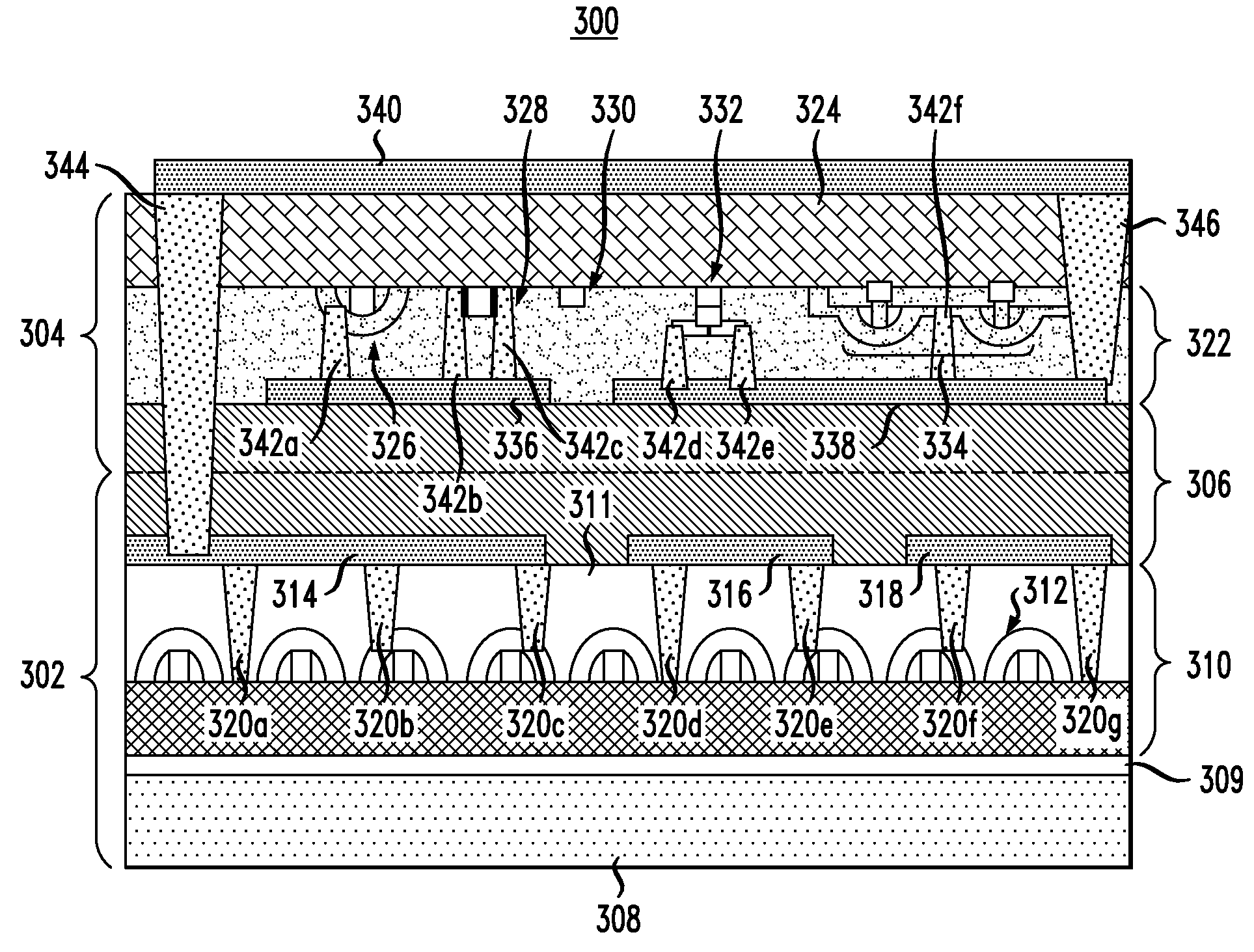
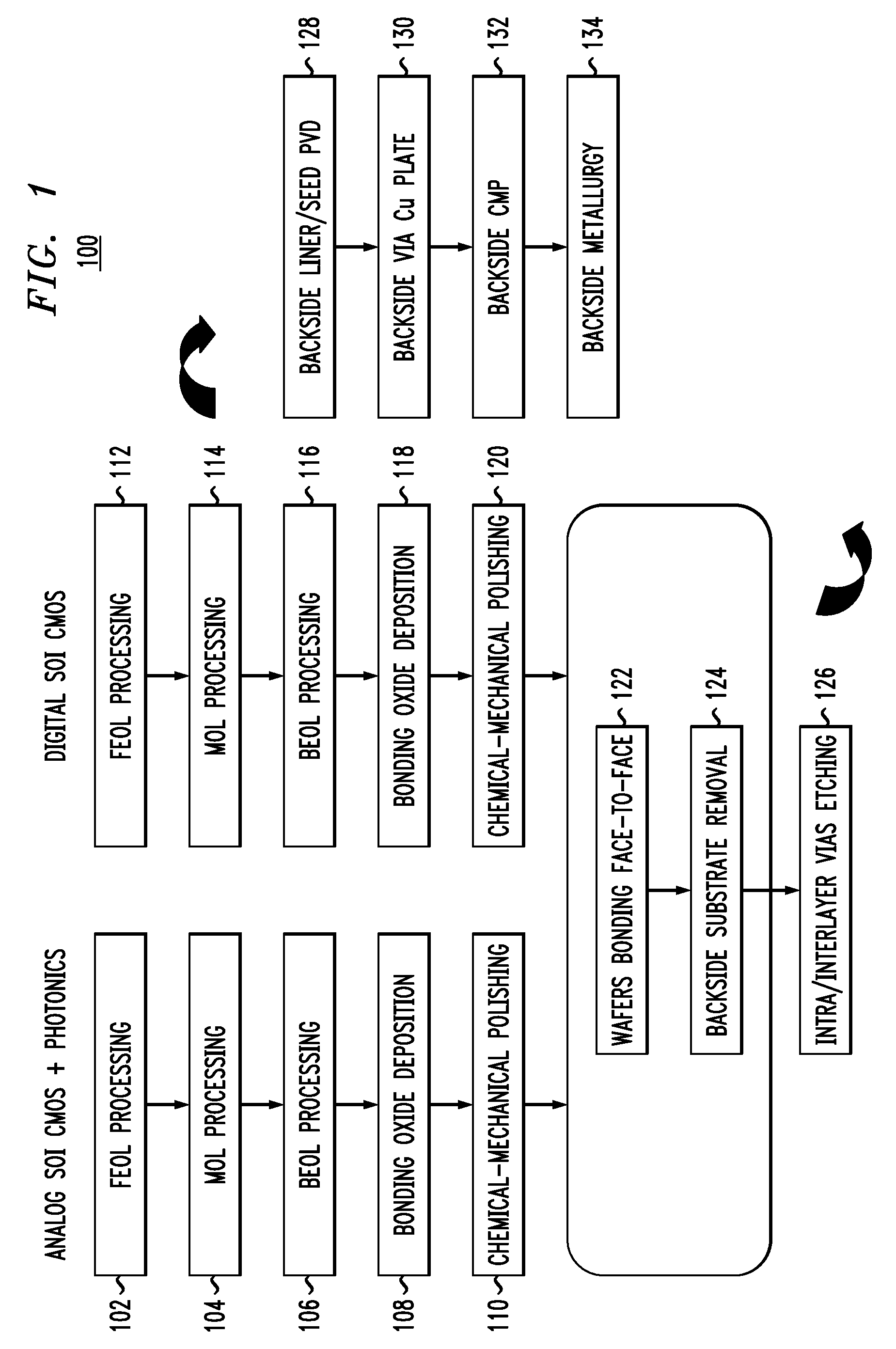
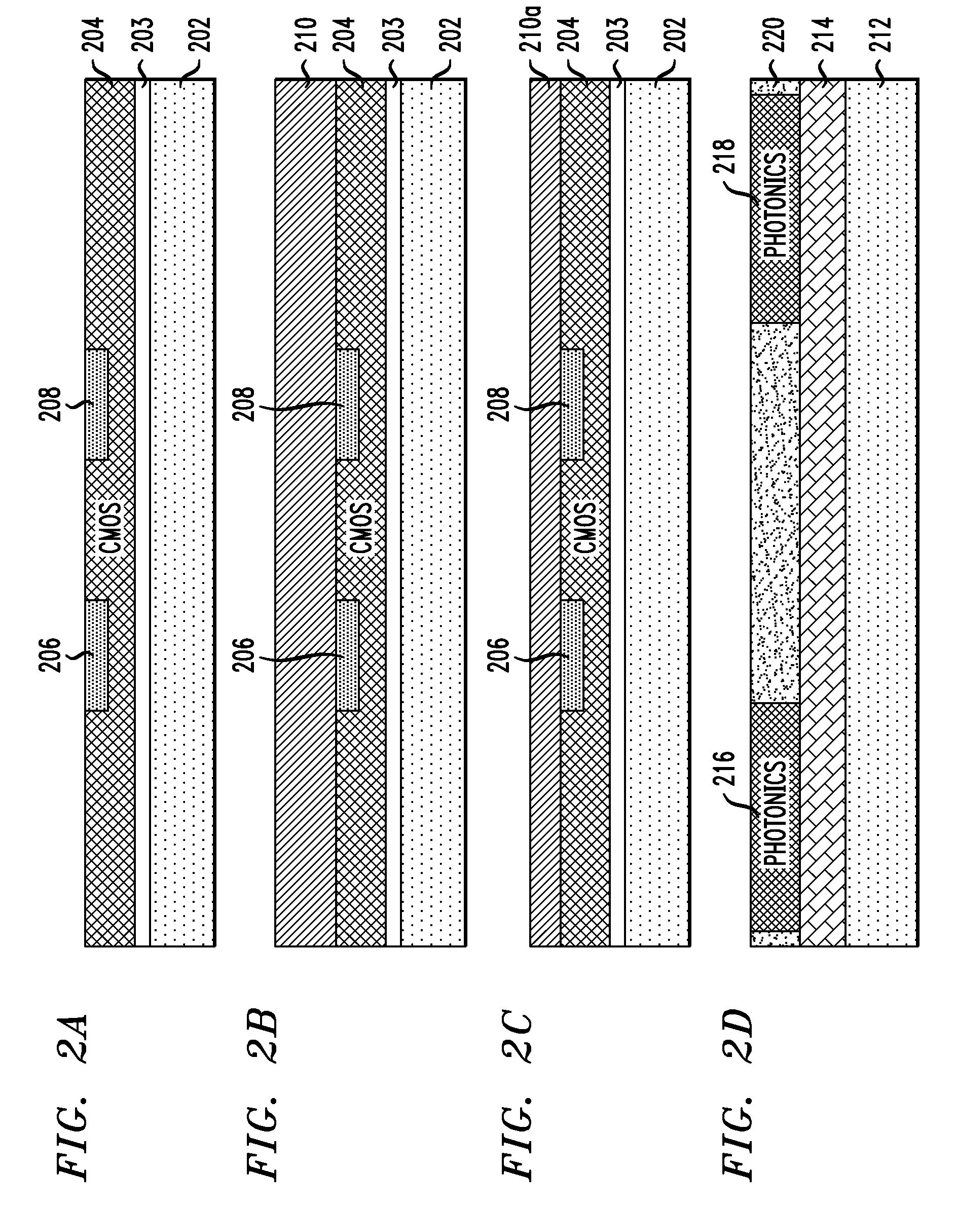
[0017]FIG. 1 is a diagram illustrating exemplary methodology 100 for fabricating a three-dimensional integrated circuit. Specifically, FIG. 1 provides an overview of a process whereby analog complementary metal-oxide semiconductor (CMOS) and photonics components (also referred to herein collectively as “analog CMOS / photonics circuitry”), fabricated on a common silicon-on-insulator (SOI) top wafer, are integrated with digital CMOS components (also referred to herein collectively as “digital CMOS circuitry”) fabricated on a common SOI or bulk-silicon (Si) bottom wafer. The designations “top” and “bottom” refer to an orientation of the wafers / device layers (see below) relative to one another in the fabricated circuit, and will be used to identify the wafers / device layers throughout the fabrication process. Further, the top wafer with analog CMOS / photonics circuitry and related components / layers is referred to hereinafter as a “top device layer,” and the bottom wafer with digital CMOS c...


PUM


Abstract

Integrated circuits having complementary metal-oxide semiconductor (CMOS) and photonics circuitry and techniques for three-dimensional integration thereof are provided. In one aspect, a three-dimensional integrated circuit comprises a bottom device layer and a top device layer. The bottom device layer comprises a substrate; a digital CMOS circuitry layer adjacent to the substrate; and a first bonding oxide layer adjacent to a side of the digital CMOS circuitry layer opposite the substrate. The top device layer comprises an analog CMOS and photonics circuitry layer formed in a silicon-on-insulator (SOI) layer having a buried oxide (BOX) with a thickness of greater than or equal to about 0.5 micrometers; and a second bonding oxide layer adjacent to the analog CMOS and photonics circuitry layer. The bottom device layer is bonded to the top device layer by an oxide-to-oxide bond between the first bonding oxide layer and the second bonding oxide layer.

Description

CROSS-REFERENCE TO RELATED APPLICATION(S)[0001]This application is related to the commonly owned U.S. application Ser. No. 12 / 132,029, entitled “Techniques for Three-Dimensional Circuit Integration,” filed herewith on the same day of Jun. 3, 2008, the contents of which are incorporated by reference herein.FIELD OF THE INVENTION[0002]The present invention relates to integrated circuits, and more particularly, to integrated circuits having complementary metal-oxide semiconductor (CMOS) and photonics circuitry and techniques for three-dimensional integration thereof.BACKGROUND OF THE INVENTION[0003]To address the scaling requirements of today's electronic devices, chip designers and manufacturers are constantly trying to devise circuit designs that best maximize available chip space. The resulting designs often extend to several different planes. For example, one such three-dimensional circuit design might involve a number of different device layers oriented in a stacked configuration....

Claims


Application Information

Patent Timeline
Patent Type & Authority Patents(United States)
IPC IPC(8): H01L27/12
CPCH01L25/167H01L27/0688H01L27/144H01L2224/83894H01L2224/9202H01L2224/9212H01L2224/80896H01L2224/8203H01L2224/821H01L2224/80001H01L2224/82
Inventor ASSEFA, SOLOMONCHEN, KUAN-NENGKOESTER, STEVEN J.VLASOV, YURII A.
Owner GLOBALFOUNDRIES US INC
Learn More