Solid-state photodetector pixel and photodetecting method

a photodetector and solid-state technology, applied in the field of solid-state photodetecting, can solve the problem that the standard ccd pixels may not be sufficient, and achieve the effect of higher shutter efficiency and higher sensitivity

Active Publication Date: 2011-03-01
AMS SENSORS SINGAPORE PTE LTD
View PDF6 Cites 21 Cited by
  • Summary
  • Abstract
  • Description
  • Claims
  • Application Information

AI Technical Summary

Benefits of technology

[0005]It is an object of the invention to provide a photodetector pixel and a photodetecting method which provide a higher shutter efficiency and a higher sensitivity.
[0011]The method according to the invention for detecting incident electromagnetic radiation, comprises the steps of converting the incident electromagnetic radiation into charge carriers of a first and a second charge type in an active region of a semiconductor material with a plane surface, generating a lateral electric potential across the active region, and storing outside the active region charge carriers of at least one type generated in the active region. Charge separation in the active region and charge transport from the active region to the charge-storage means is additionally enhanced.

Problems solved by technology

For such special applications, the properties of standard CCD pixels may not be sufficient.

Method used


Image

  • Solid-state photodetector pixel and photodetecting method
  • Solid-state photodetector pixel and photodetecting method
  • Solid-state photodetector pixel and photodetecting method

Examples


first embodiment

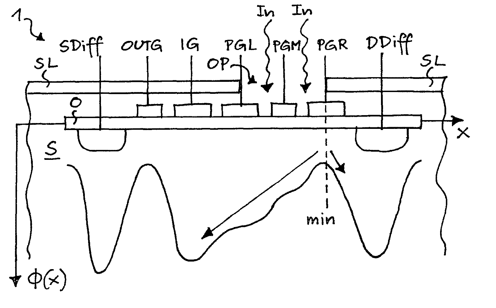
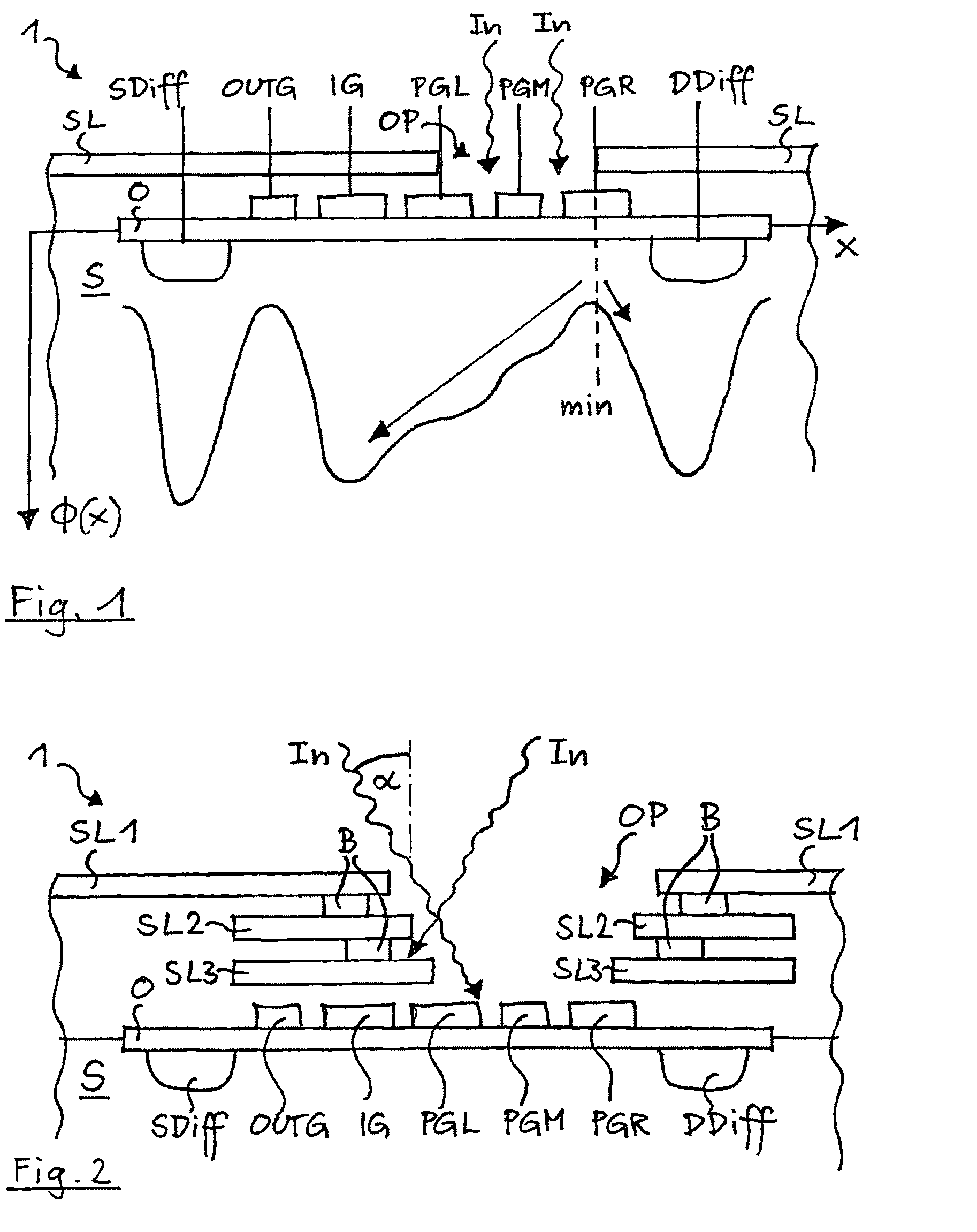
[0031]FIG. 1 shows a cross-sectional view of a CCD part of a photodetector pixel 1 according to the invention. The pixel 1 comprises the well-known structures such as a left photogate PGL, a middle photogate PGM and a right photogate PGR. The region beneath the photogates PGL, PGM and PGR can be called the “active region” of the pixel, since this is the region in which incident radiation In is converted into charge carriers. The pixel 1 further comprises either at least one integration gate (IG) for storing charge carriers generated in the active region and at least one dump site (DDiff), or at least two integration gates, the integration gates (IG) and the dump-site (DDiff) being placed outside the active region. The embodiment of FIG. 1 comprises an integration gate IG, an isolation gate OUTG, a sense diffusion SDiff and a dump diffusion DDiff. All these elements PGL, PGM, PGR, IG, OUTG, SDiff, DDiff are arranged above or beneath a gate-oxide layer O on a substrate S made of, e.g....

second embodiment

[0034]It has been found that a shielding layer SL as shown in FIG. 1 shields well in case of normal incidence (α=0) of light on the pixel, but not in other cases, and especially not for large incidence angles α of, e.g., 15° and more. This is due to the three-dimensional geometric arrangement of the gates and the shielding layer SL. The latter is placed about 4 μm (depending on the used process) above the surface of the substrate S, so that light In impinging at an angle α≠0 reaches, e.g., part of the integration gate IG. This is avoided in a pixel according to the invention, shown in FIG. 2. This embodiment uses, besides a topmost shielding layer SL1, other metal layers SL2, SL3, . . . , which lie closer to the substrate S as further shielding layers. Such metal layers SL2, SL3, . . . are provided, e.g., in a standard complementary-metal-oxide-semiconductor (CMOS) process for interconnecting lines. The lowermost metal layer SL3, which lies typically about 1 μm above the surface of ...

third embodiment

[0049]a photodetecting method according to the invention also relates to a TOF range camera comprising a plurality of photosensitive areas. This method allows to control whether a pixel 1 is intact and works correctly. The idea is to create redundancy by performing at least two measurements of the same scene, however, with different phases of the emitted CW-modulated light. A phase shift of δ (in degrees) introduces an artificial distance shift of

[0050]Δ⁢⁢L=δ360⁢°·c2⁢f,

wherein c≈3·108 m / s is the light velocity in air and f is the modulation frequency. In an example where f=20 MHz and δ=180°, an artificial distance shift of ΔL=3.75 m should be obtained. If this is not the case for a certain pixel, said pixel is faulty.

[0051]Another preferred field of application of the pixel according to the invention is (bio-)chemical sensing. Some examples for such applications are given in the following.

[0052]A first application concerns (bio-)chemical sensors using luminescent labels. Two general...


PUM

PropertyMeasurementUnit
thicknessaaaaaaaaaa
thicknessaaaaaaaaaa
incidence anglesaaaaaaaaaa

Abstract

A pixel is formed in a semiconductor substrate (S) with a plane surface for use in a photodetector. It comprises an active region for converting incident light (In) into charge carriers, photogates (PGL, PGM, PGR) for generating a lateral electric potential (Φ(x)) across the active region, and an integration gate (IG) for storing charge carriers generated in the active region and a dump site (Ddiff). The pixel further comprises separation-enhancing means (SL) for additionally enhancing charge separation in the active region and charge transport from the active region to the integration gate (IG). The separation-enhancing means (SL) are for instance a shield layer designed such that for a given lateral electric potential (Φ(x)), the incident light (In) does not impinge on the section from which the charge carriers would not be transported to the integration gate (IG).

Description

[0001]This application is a §371 national phase filing of PCT / CH2005 / 000436 filed Jul. 25, 2005, and claims priority to European application No. 04 405 475.7 filed Jul. 26, 2004.FIELD OF THE INVENTION[0002]This invention relates to solid-state photodetecting, especially charge-coupled-device (CCD) photodetecting. In particular, it relates to a photodetector pixel and a photodetecting method according to the preambles of the independent claims. Possible applications of the invention lie, for instance, in range detection or in (bio-)chemical sensing.BACKGROUND OF THE INVENTION[0003]Solid-state one-dimensional and two-dimensional photodetectors with picture elements (pixels) based on the charge-coupled-device (CCD) principle are well-known; cf. A. J. P. Theuwissen: “Solid State Imaging with Charge Coupled Devices”, Kluwer Academic Publishers, Dordrecht, 1995. They find use not only in consumer goods such as ordinary cameras, but also in combination with a dedicated light source in spec...

Claims


Application Information

Patent Timeline
Patent Type & Authority Patents(United States)
IPC IPC(8): G01T1/24H01L27/148G01N21/64G01S17/894H01L27/146
CPCH01L27/14601H01L27/14623H01L31/0232H01L31/02005H01L27/148G01S17/894G01N21/648
Inventor KAUFMANN, ROLFOGGIER, THIERRYNEUKOM, SIMONLEHMANN, MICHAEL
Owner AMS SENSORS SINGAPORE PTE LTD
Why Eureka
Try Eureka