
Light emitting device and electronic apparatus

a technology electronic devices, which is applied in the direction of solid-state devices, semiconductor devices, printing, etc., can solve the problems of deterioration of characteristics, decrease in resolution, and decrease in the intensity of light output of light emitting devices, and achieve high image quality

Active Publication Date: 2011-03-08
SEIKO EPSON CORP
View PDF4 Cites 0 Cited by
  • Summary
  • Abstract
  • Description
  • Claims
  • Application Information

AI Technical Summary

Benefits of technology

This configuration maintains the original light emission shape, increases light detection sensitivity, and ensures uniform luminance distribution, improving the overall performance and image quality of the light emitting device.

Problems solved by technology

However, under the configuration in which the light detecting element is disposed to be overlapped with the light emitting element, there is a problem that the intensity of light output from the light emitting device decreases.
Thus, there is a problem that deterioration of characteristics such as a decrease in the resolution occurs due to asymmetry of the shape of the light emitting area.

Method used


Image

  • Light emitting device and electronic apparatus
  • Light emitting device and electronic apparatus
  • Light emitting device and electronic apparatus

Examples


first embodiment

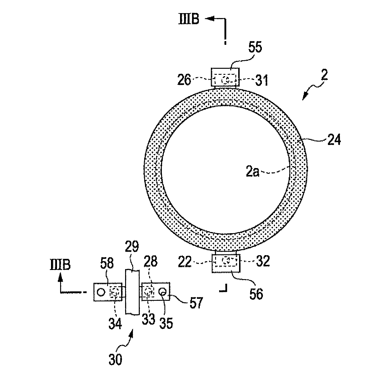
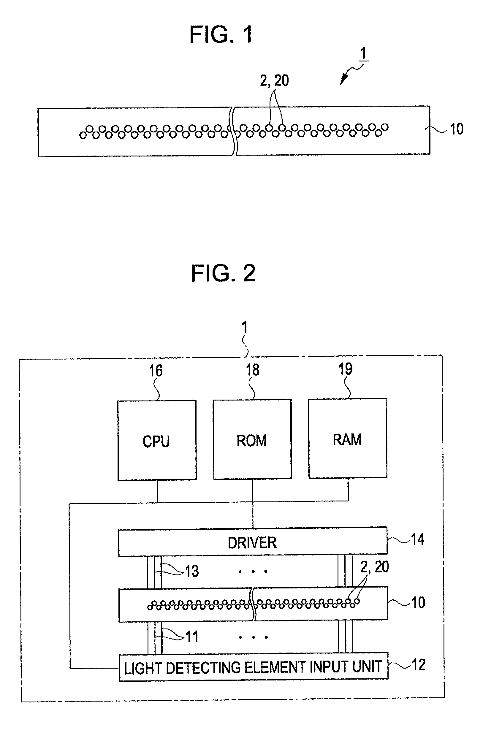
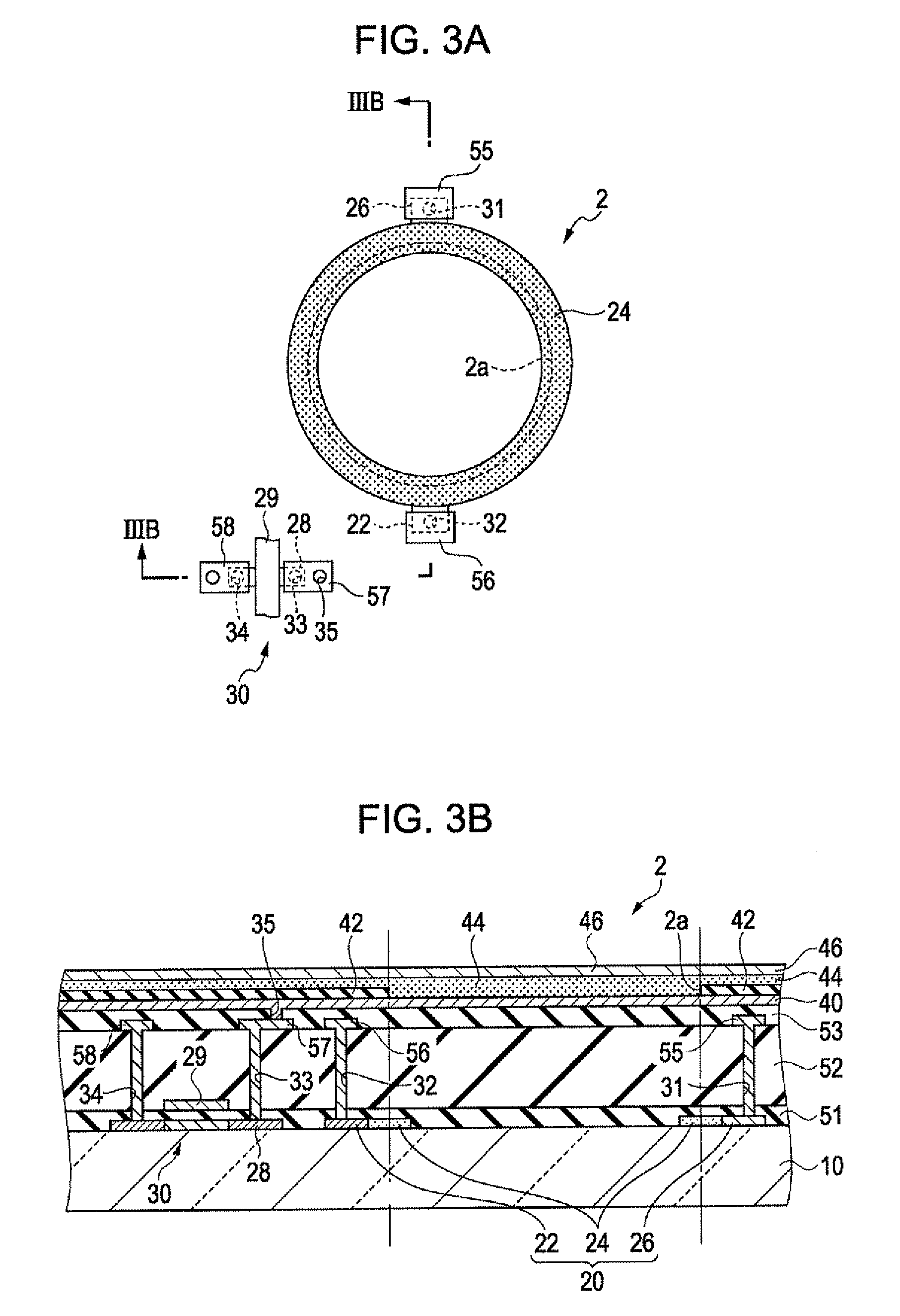
[0038]FIG. 1 is a plan view of an organic EL device 1 as a light emitting device. The organic EL device 1 is configured to have a substrate 10 having transparency as a base body. The organic EL device 1 has a plurality of light emitting elements 2 that are formed to form a row on the substrate 10. Each light emitting element 2 is electrically connected to a drain of a thin film transistor (hereinafter, abbreviated as a TFT) element 30 (FIG. 3B) and emits light having light intensity corresponding to the magnitude of a current flowing through the TFT element 30. To a gate of the TFT element 30, a first capacitor element (not shown) is electrically connected.

[0039]In addition, on the substrate 10, a light detecting element 20 is formed near each light emitting element 2. The light detecting element 20 is configured to include a pin diode having a p-type semiconductor layer 22, a sensitivity area 24, and an n-type semiconductor layer 26 (FIG. 3). In addition, the light detecting elemen...

second embodiment

[0063]Subsequently, a second embodiment of the invention will be described. According to this embodiment, an area included in the light detecting element 20 for forming the sensitivity area 24 is different from that according to the first embodiment, and other configurations and advantages of the configurations are the same as those according to the first embodiment. Hereinafter, the second embodiment will be described with a difference between the first and second embodiments primarily focused.

[0064]FIGS. 4A and 4B are diagrams showing a light emitting element 2 and a light detecting element 20 according to the second embodiment. FIG. 4A is a plan view, and FIG. 4B is a cross-section view taken along line IVB-IVB shown in FIG. 4A. As shown in FIG. 4A, in this embodiment, the light detecting element 20 is formed on an outer side of the light emitting element 2 in a plan view, and the outer frame 2a of the light emitting element 2 coincides with a part of the outer frame of the light...

third embodiment

[0066]Subsequently, a third embodiment of the invention will be described. In this embodiment, areas for forming the p-type semiconductor layer 22 and the n-type semiconductor layer 26 of the light detecting element 20 are different from those of the first embodiment, and other configurations and advantages of the configurations are the same as those according to the first embodiment. Hereinafter, the third embodiment will be described with a difference between the first and third embodiments primarily focused.

[0067]FIGS. 5A and 5B are diagrams showing a light emitting element 2 and a light detecting element 20 according to the third embodiment. FIG. 5A is a plan view, and FIG. 5B is a cross-section view taken along line VB-VB shown in FIG. 5A. As shown in FIG. 5A, in this embodiment, the p-type semiconductor layer 22 of the light detecting element 20 is formed along the outer frame 2a of the light emitting element 2 in an area overlapped with the light emitting element 2 in a plan ...


PUM


Abstract

A light emitting device includes a substrate having transparency, a light emitting element that emits light at least to the substrate side, and a light detecting element that is formed between the light emitting element and the substrate. The light detecting element is formed along an outer frame of the light emitting element in a plan view.

Description

BACKGROUND[0001]1. Technical Field[0002]The present invention relates to a light emitting device and an electronic apparatus.[0003]2. Related Art[0004]As one of image forming apparatuses such as printers and facsimiles, a device that uses a light emitting device as an exposure head has been known. As the light emitting device, for example, an organic EL (Electro Luminescence) device having light emitting elements disposed so as to form a row can be used. In such a case, it is preferable that the intensity of light emitted from the light emitting elements is uniform.[0005]In JP-A-2007-290329 and JP-A-2002-178560, technology in which a light detecting element for detecting light emitted from a light emitting device is disposed in a light emitting device and the intensity of light emitted from the light emitting element is corrected to a predetermined value based on the result of detection by using the light detecting element has been disclosed. Between these, in JP-A-2007-290329, a co...

Claims


Application Information

Patent Timeline
Patent Type & Authority Patents(United States)
IPC IPC(8): H01L33/00B41J2/44B41J2/45B41J2/455H01L31/10H01L51/50H04N1/036
CPCB41J2/45H01L27/3269H01L27/326H10K59/121H10K59/13
Inventor EGUCHI, TSUKASAJO, HIROAKIKANDA, EIJIKASAI, TOSHIYUKIITO, ATSUSHI
Owner SEIKO EPSON CORP
Learn More