Temporary-fixing substrate and method for molding electronic component

a technology of temporary fixing substrate and electronic components, which is applied in the direction of basic electric elements, electrical apparatus, semiconductor/solid-state device details, etc., can solve the problems of low light reaching the interface between the temporary fixing substrate and electronic parts, low yield of separation in many cases, and unique problems, so as to achieve easy incident into the substrate and easy separation

Inactive Publication Date: 2020-01-23
NGK INSULATORS LTD
View PDF0 Cites 0 Cited by
  • Summary
  • Abstract
  • Description
  • Claims
  • Application Information

AI Technical Summary

Benefits of technology

[0021]Light is then irradiated onto the bottom face of the temporary-fixing substrate. As the scratches are decreased on the bottom face and the polished surfaces of the crystal grains and grain boundaries are exposed to the bottom face, the light is relatively easily made incident into the

Problems solved by technology

However, in the case that a plurality of the electronic parts is adhered and then temporary-fixed on the temporary-fixing substrate with the resin mold and that the electronic parts are separated from the temporary-fixing substrate by light irradiation. unique problems are proved to be provided.
However,

Method used


Image

  • Temporary-fixing substrate and method for molding electronic component
  • Temporary-fixing substrate and method for molding electronic component
  • Temporary-fixing substrate and method for molding electronic component

Examples


##ventive example 1

Inventive Example 1

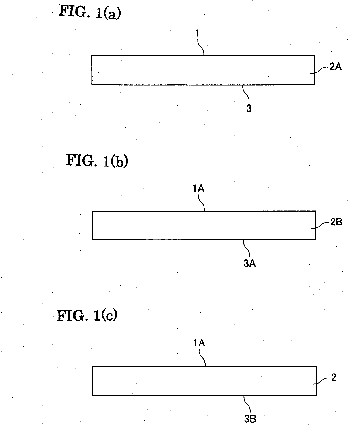
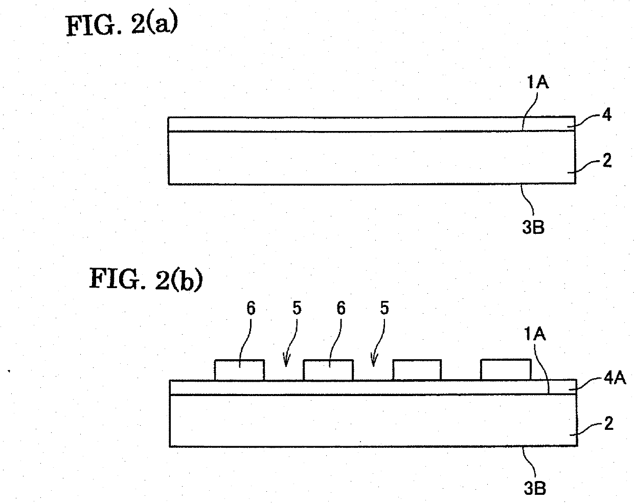
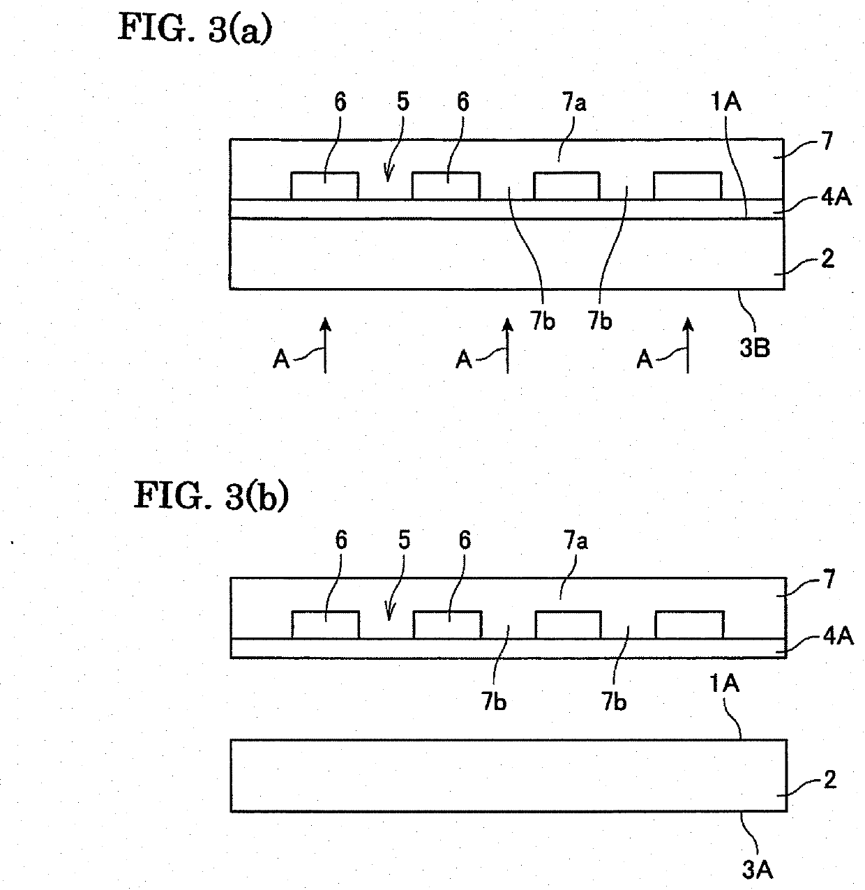
[0060]It was produced the temporary-fixing substrate, and the electronic parts and resin mold were separated from the temporary-fixing substrate, as shown in FIGS. 1 to 3.

[0061]Specifically, it was produced slurry by mixing the following components.

(Powdery Raw Material)

[0062]α-alumina powder having a specific surface area of 3.5 to 4.5 m2 / g and an average primary particle size of 0.35 to 0.45 μm

100 weight partsMgO (magnesia)0.025 weight partsZrO2 (zirconia)0.040 weight partsY2O30.0015 weight parts 

(Dispersing Medium)

[0063]

Dimethyl glutarate 27 weight partsEthylene glycol0.3 weight parts

(Gelling Agent)

[0064]

MDI resin4 weight parts

(Dispersing Agent)

[0065]

High molecular surfactant3 weight parts

(Solvent)

[0066]

N,N-dimethyl amino hexanol0.1 weight parts

[0067]The slurry was injected into a mold of aluminum alloy at room temperature and then stood for 1 hour at room temperature. The slurry was then stood at 40° C. for 30 minutes to proceed the solidification and then rel...

##ventive example 2

Inventive Example 2

[0073]It was produced the temporary-fixing substrate and the electronic parts and resin mold were separated from the temporary-fixing substrate, according to the same procedure as those in the Inventive Example 1. However, the time period of performing the chemical mechanical polishing of the bottom face was shortened so that the line number of the scratches observed in the visual field was made 5 lines. As a result, the yield of the separation of the electronic parts and resin mold was proved to be 99.3%.

##ventive example 3

Inventive Example 3

[0074]It was produced the temporary-fixing substrate, and the electronic parts and resin mold were separated from the temporary-fixing substrate, according to the same procedure as the inventive Example 1. However, the time period of the chemical mechanical polishing of the bottom face is made longer, so that the line number of the scratches observed in the visual field was proved to be 0. As a result, the yield of the separation of the electronic parts and resin mold was proved to be 99.5%.


PUM


Abstract

A temporary-fixing substrate includes a fixing face for adhering and temporary-fixing a plurality of electronic parts with a resin mold and a bottom face on the opposite side of the fixing face. The temporary-fixing substrate is composed of a translucent ceramic material, scratches are distributed on the fixing face, and intergranular boundaries and polished surfaces of crystal grains forming the translucent ceramic material are exposed to the bottom face. The density of scratches on the bottom face is lower than the density of scratches on the fixing face.

Description

CROSS-REFERENCE TO RELATED APPLICATIONS[0001]This application is a continuation application of PCT / JP2018 / 003404, filed Feb. 1, 2018, which claims priority to Japanese Application No. 2017-066793, filed Mar. 30, 2017, the entire contents all of which are incorporated hereby by reference.TECHNICAL FIELD[0002]The present invention relates to a temporary-fixing substrate including a fixing face for adhering and temporary-fixing electronic parts with a resin mold and a bottom face on the opposite side of the fixing face.BACKGROUND ARTS[0003]It is known a method of adhering and fixing electronic parts made of silicon or the like on a supporting body made of a glass or ceramic (Patent documents 1, 2 and 3). According to such related arts, electronic parts are adhered to a supporting body with a thermal curable resin and then cooled to obtain a bonded body. In this case, it is tried to adjust the warpage of the supporting body to reduce the warpage of the bonded body. Further, the warpage ...

Claims


Application Information

Patent Timeline
IPC IPC(8): H01L21/56H01L21/321
CPCH01L21/3212H01L21/565H01L21/568H01L21/561H01L21/304H01L23/28H01L23/15
Inventor NOMURA, MASARUMIYAZAWA, SUGIO
Owner NGK INSULATORS LTD
Why Eureka
Try Eureka